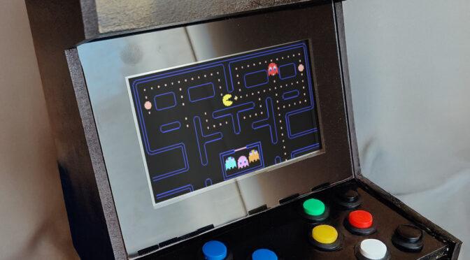
Since I’ve been working on home automation, I’ve naturally wanted to optimize and simplify as much as possible and adapt and implement it in line with the new buzzwords “green electronics”, “sustainability”, “energy-saving” … and so on. For example, my appliances switch off when they are not used or ignored, stand-by energy consumption is largely avoided and IOT technology also prevents human forgetfulness (leaving windows open in winter or forgetting to switch lights off). As readers of the blog already know, I use systems such as HomeMatic, NodeRed and, for some time now, Homeassistant with ESPHome, Zigbee2Mqtt etc. Of course, the aim is also to keep all systems cloud-free. I don’t want the data to take a detour via some server in the Far East to switch a light on and off in my home. So, if possible, everything should take place within my own network and not “phone” to the outside and also work if I cut the data line.
For a long time now, various suppliers have been offering an extremely practical device for comfort in the parents’ quiet room. I’m talking about a space-saving way of accommodating the flicker box (nowadays also known as a flat-screen TV) in the room. I’m just mentioning terms like:
Speaka Professional TV ceiling mount electric motorized (1439178) or MyWall HL46ML … etc. Some of these devices can be controlled with a wireless remote control, others via the Tuya CloudApp. You can bypass the Tuya app via the Tuya IOT development environment and bring these devices into your home assistant via the “TuyaLocal” integration – it works – but it’s more of a “ONLY” solution. In my opinion, the ideal solution is to integrate these devices into the ESPHome system. Using the Speaka Professional TV ceiling mount as an example, I will show you how it can be integrated into the ESPHome network and thus into the Home Assistant with a small extension. This version of the SpeaKa part has no Internet connection and is only controlled via a wireless remote control.
TV ceiling mount with open cover
With a little reverse engineering, we (my colleague Werner and myself) analyzed the existing appliance factory. The system is structured something like this:
Circuit board in the ceiling bracket
Systemdiagramm
The system diagram above shows how the circuit board is constructed. The power supply comes from a plug-in power supply with DC 24V output at 1.5A. On the board you can still see an unpopulated area whose solder pads are wired with +3V3, GND and RX, TX lines suitable for an ESP8266. A USB socket can also be seen. These two interfaces are not included in the diagram. We examined the RX/TX lines that are routed from the unpopulated solder pads (ESP8266) to the microcontroller (1301 X 016B). However, no signals could be measured here. (Presumably the interface is not activated in the flashed program version).
“Debug” wires on the RX/TX and on the RF chip
So this does not take us any further. In the next step, we looked at where the control signals of the radio remote control come from and how they are subsequently implemented. The RF receiver chip has 16 pins and unfortunately no labeling. Or has it been removed? The supply voltage of the RF chip is connected to pin 1 and pin 16, pin 2 and pin 3 are connected to a crystal and a line is routed from pin 9 to the microcontroller. So this must be the data output. Using the “PulseView” software from Sigrok and a Far East logic analyzer, we sniffed this output. And lo and behold, data packets with a duration of 10.3ms were revealed here. The PulseView software was able to recognize the protocol as an RS232 protocol after a few attempts with different analyzed data rates. It was then easy to log the received and decoded control commands to the microcontroller.
RF chip with connected “sniffer” cable
The baud rate of the RS232 port on the RF chip output is 9600 at 8N1. 10 bytes are received in HEX for each command sent. Here is the list of commands: (missing bytes follow…maybe sometime)
Befehl
Byte0
Byte1
Byte2
Byte3
Byte4
Byte5
Byte6
Byte7
Byte8
Byte9
UP
0xAA
0x06
0x04
0x25
0x03
0xD5
0x01
0x00
0x02
0x55
DOWN
0xAA
0x06
0x04
0x25
0x03
0xD5
0x00
0x10
0x11
0x55
LEFT
0xAA
0x06
0x04
0x25
0x03
0xD5
0x55
RIGHT
0xAA
0x06
0x04
0x25
0x03
0xD5
0x55
BUTTON1
0xAA
0x06
0x04
0x25
0x03
0xD5
0x55
BUTTON2
0xAA
0x06
0x04
0x25
0x03
0xD5
0x00
0x08
0x09
0x55
MEM1
0xAA
0x06
0x04
0x25
0x03
0xD5
0x55
MEM2
0xAA
0x06
0x04
0x25
0x03
0xD5
0x55
OK
0xAA
0x06
0x04
0x25
0x03
0xD5
0x00
0x40
0x41
0x55
SET
xx
xx
xx
xx
xx
xx
xx
xx
xx
xx
Once the data protocol had been found using the logic analyzer, we tried to send the data to the microcontroller using a terminal program and a USB to TTL232 converter. The RF chip was removed for this purpose. It pulled the level to VCC in the idle state and prevented parallel operation of the “RS232 transmitter”.
RF-Chip removedBoard without chip with debug line
USB UART for sending commands
The control commands from the table above could be successfully sent via the terminal program. Now only an ESP32 board had to take over this task. An ESP32 NodeMCU board from the pool was equipped with a basic ESPHome image and integrated into the Homeassistant network. The ESPHome node now only had to be taught to send the byte sequence via the TX pin of the ESP32 when the corresponding trigger was activated in the Homeassistant. To do this, the ESP32 board was attached to the PCB and the VCC3V3, GND and TX lines were soldered to PIN9 of the former RF chip.
ESP32 on the board of the Speaka ceiling bracket
Re-installed in the ceiling bracket
The following esphome script must now be added to the ESPHome web environment.
esphome:
name: tvhalterung
friendly_name: TVHalterung
esp32:
board: esp32dev
framework:
type: arduino
# Enable logging
logger:
# Enable Home Assistant API
api:
encryption:
key: "hier dein key beim Anlegen des device"
ota:
password: "hier dein ota password"
wifi:
ssid: !secret wifi_ssid
password: !secret wifi_password
# Enable fallback hotspot (captive portal) in case wifi connection fails
ap:
ssid: "Tvhalterung Fallback Hotspot"
password: "hier wieder deins"
captive_portal:
uart:
tx_pin: 4
rx_pin: 5
baud_rate: 9600
# Example button configuration
button:
- platform: template
name: TV Halterung UP
id: tv_up
icon: "mdi:arrow-up-bold-outline"
on_press:
- logger.log: "Button pressed TV Up"
- uart.write: [0xAA,0x06,0x04,0x25,0x03,0xD5,0x01,0x00,0x02,0x55]
- platform: template
name: TV Halterung OK
id: tv_ok
icon: "mdi:stop-circle-outline"
on_press:
- logger.log: "Button pressed TV OK"
- uart.write: [0xAA,0x06,0x04,0x25,0x03,0xD5,0x00,0x40,0x41,0x55]
- platform: template
name: TV Halterung DOWN
id: tv_down
icon: "mdi:arrow-down-bold-outline"
on_press:
- logger.log: "Button pressed TV Down"
- uart.write: [0xAA,0x06,0x04,0x25,0x03,0xD5,0x00,0x10,0x11,0x55]
- platform: template
name: TV Halterung Button1
id: tv_button1
icon: "mdi:numeric-1-circle-outline"
on_press:
- logger.log: "Button pressed TV Button1"
- uart.write: [0xAA,0x06,0x04,0x25,0x03,0xD5,0x00,0x20,0x21,0x55]
- platform: template
name: TV Halterung Button2
id: tv_button2
icon: "mdi:numeric-2-circle-outline"
on_press:
- logger.log: "Button pressed TV Button2"
- uart.write: [0xAA,0x06,0x04,0x25,0x03,0xD5,0x00,0x08,0x09,0x55]
- platform: template
name: TV Halterung Left
id: tv_left
icon: "mdi:arrow-left-bold-outline"
on_press:
- logger.log: "Button pressed TV Left"
- uart.write: [0xAA,0x06,0x04,0x25,0x03,0xD5,0x00,0x20,0x21,0x55]
- platform: template
name: TV Halterung Right
id: tv_right
icon: "mdi:arrow-right-bold-outline"
on_press:
- logger.log: "Button pressed TV Right"
- uart.write: [0xAA,0x06,0x04,0x25,0x03,0xD5,0x00,0x20,0x21,0x55]
- platform: template
name: TV Halterung MEM1
id: tv_mem1
icon: "mdi:alpha-m-circle-outline"
on_press:
- logger.log: "Button pressed TV MEM1"
- uart.write: [0xAA,0x06,0x04,0x25,0x03,0xD5,0x00,0x01,0x02,0x55]
- platform: template
name: TV Halterung MEM2
id: tv_mem2
icon: "mdi:alpha-m-circle-outline"
on_press:
- logger.log: "Button pressed TV MEM2"
- uart.write: [0xAA,0x06,0x04,0x25,0x03,0xD5,0x00,0x01,0x02,0x55]
Once the esphomescript has been compiled and uploaded to the ESP, there is a new ESPHome device with the name TV holder in the Home Assistant environment. The buttons for the control are now listed here as entities. If everything went well, you should now be able to control the TV mount via the Home Assistant.
(Not all control commands have been implemented correctly yet – the correct codes will be added to the table)
In the article “Pylontech PV battery status in HomeAssistant”, I had improved the project “Pylontech battery monitoring” of the following GitHub links and drew a circuit board to make the whole construct a little more compact and professional. https://github.com/irekzielinski/Pylontech-Battery-Monitoring https://github.com/hidaba/PylontechMonitoring
All battery data of the Pylontech battery modules are displayed in the Homeassistant. Great! But when I take a look at the list of devices registered in my wifi networks, I almost feel sick – there are now far too many wireless devices, especially from the smart home sector, sharing the channel bandwidth. So my current plan is to bring some of the smart home devices onto the wired LAN network.
The self-made devices based on the ESPs are ideal for this. These are devices such as the OpenDTU interface, the EVU smart home interface or, as here, the interface from the serial console of the Pylontech battery to the MQTT server in the Home Assistant.
I have done some tests with boards such as the OLIMEX ESP32-PoE and the WT32-ETH01. The Olimex board would have the great advantage of also being able to be supplied with power via PoE. However, the power supply for PoE operation is so “poor” that the required standards of external boards are not met. Here I can mention the NRF24L01 radio module, for example. I did some tests with it and decided to disregard the PoE functionality for the time being. This led to the plan to use the WT32-ETH01 with an ESP32 to design a universal board with several interfaces. It should be able to do the following:
communicate with the PV inverters using OpenDTU and NRF24L01
communicate with the Smarthome system via the Pylontech Console using MQTT
have an optional CAN interface
be able to communicate via RS422/RS485 in addition to the RS232 interface
receive the power supply via 5V USB
and to have everything packed nicely small and compact in one housing
So I designed a circuit and drew a circuit board. I got the boards manufactured by a Far East PCB manufacturer. The assembly is also done quickly.
Circuit diagram of the Universal Lan Interface
The picture below shows the PCB layout before production.
The WT32-ETH01 board does not have a USB port for programming the controller. It is programmed via an external USB-UART adapter. To activate the programming mode, an IO pin must also be connected to GND. To simplify this somewhat, there is now a “PROG” jumper on the board. If this jumper is plugged in, the WT32 can receive the firmware files. I have provided a pin header slot “TO-FTDI” as a connection option for the USB-UART adapter.
The board is now designed that it can be used to operate different devices. If you connect an NRF24L01 module to the “NRF24L01+” pin header and flash the ESP32-OpenDTU image to the controller, the inverter data can be received and transmitted via the LAN network. I have created a suitable IO-config jason-file for the use of the WT32.
Another application is the use of the board with the serial output of the battery data of the Pylontech PV batteries. The batteries provide a “Console” port which represents an RS232 interface. The data is transferred to the WT32 controller via this port and is then available via LAN in the local network.
I have adapted the ESP8266 script from hidaba and irekzielinski for the ESP32 controller. (see code at the end of the article)
Once the code has been compiled and uploaded, the status of the Pylontec batteries should be visible under the set IP address after all connections have been made.
Board version with Pylontech setupVersion with OpenDTU and NRF24L01 setup
The device setups shown in the picture are equipped with a housing. I have published the “.stl” files created with FreeCad on thingiverse.
Little by little, I am bringing many of my smarthome components to a common standard. I have decided to bring all devices together via a NodeRed server. The HomeMatic system also communicates with NodeRed. Among other things, I also transfer the measured values of the EVU meter (I have a Siemens IM350 smart meter installed) to the HomeMatic CCU. This is done as mentioned in an earlier post, via the LED pulse interface (1000 pulses/kWh). For this purpose, a phototransistor is simply attached above the LED on the meter, which detects the flashing pulses of the LED and converts them into the instantaneous power in the meter sensor transmitter unit HM-ES-TX-WM and integrates them over time and then sends the data on to the CCU. This works quite well in itself. Only the update rate (in the minute range) is too long for me. Also, the phototransistor seems to react again and again to the stray light of the neighboring LED (which displays the reactive power in 1000 pulses/kvarh). This causes discrepancies between the count via the HomeMatic sensor and the values read directly from the meter.
This is definitely more accurate. If you look at the IM350 Smartmeter meter in detail, or read through the manual, you will quickly see that it has a so-called “customer interface”. This customer interface provides some measurement data via a galvanically isolated data line every second. This includes, among others, the momentary active power in both directions, as well as the meter readings of active and reactive power in the reference and feed-in direction. So perfect starting conditions to replace the HomeMatic meter sensor with my own design. After a little Internet research, I quickly realized that I am not the only one who deals with exactly this issue. The data of the customer interface tumbles out after request over a data request line with a speed of 115kbaud. However, they are encrypted, and not directly readable. To obtain the 16-byte decryption key, the utility must be consulted. The key is tied to the smart meter serial number and is unique to each smart meter. After some phone calls with my Carinthian energy provider, the key code was sent to me by mail. In the next step I tested with a USB-UART adapter on a PC, if data really come out of the meter when the interface is wired correctly. For this I crimped a RJ11 connector to a suitable 6pin cable and wired the open end of the cable according to the datasheet of the meter. Not much is needed for this. A 5V supply must activate the interface, likewise the Data Request line must be switched to 5V and already the data packets are available at the Data Out line. By the way, it also works with a 3V3 supply. With a terminal program on the PC (I usually use putty or hterm) you can visualize the encrypted data.
Now it was time to think about how to decode and process the data. For this, one finds two approaches with net:
* via a RaspberryPi, with a Python environment and a Python script. The scripts here take over the reception and decryption of the data and then make them available for further processing in different ways
* via an ESP32. The ESP is also able to decode a 128Bit AES encryption and still has plenty of resources to process the data and send it via WiFi. Furthermore, an ESP is available in sufficient quantities for little money. So I decided to use this solution. There is an open source project on GitHub from the user https://github.com/Andre-Schuiki/esphome_im350 in which he provides an ESP32 IM350 decoder as a basis for own projects. With his sources you get a decoder that reads the meter data every second and outputs it via the USB UART programming interface and also via Telnet over WiFi. I used this source as a basis.
My goal is to put the data obtained from the smart meter into MQTT messages and send them to my MQTT broker. From there it is then a simple matter to get them into NodeRed and the HomeMatic CCU and store them there. So I adapted the code. This involved setting the wifi connection to the router to a static IP. (are to be defined in settings.h). The readout readings, as well as the RSSI of the wifi connection, are now provided via MQTT Topics. (the IP address to the broker is also to be defined in settings.h). If you compile the code now and run it on the ESP, then it should log into the respective network. As long as the ESP is still connected to a PC, you can check what it is doing via the programming interface and a terminal. If you now connect the RJ11 plug to the customer interface of the meter, the triangle above the label “KU” should flash in the display of the meter every second. If this happens, the measured values should already be displayed in the terminal (provided that you have not forgotten to enter the KEY from the utility in secrets.h). If this also works, then a look at the MQTT broker (with e.g.: MQTT Explorer) makes sure that the messages arrive. Now the ESP can be removed from the PC.
Connection assignmentESP32 in “free-flying” test setup
I chose a very simple solution and mounted the ESP on a breadboard. The 6pin cable to the smartmeter is soldered there. On the breadboard there is room for the pull-up resistors and a NPN transistor (BC547 etc.) for inverting the data pulses. I put the board in a small plastic box, which is now only connected with a cable to the customer interface and with a USB cable to a USB power supply.
The finished structure then (or currently) looks like this. The data ends up in the MQTT broker and NodeRed visualizes it and sends it to the HomeMatic CCU.
this is how the data arrives at the MQTT brokerand can be processed in NodeRed like this
if someone is interested in the customized scripts, I can send them to you. Regarding a publication on GitHub, I have to find out first which license conditions have to be fulfilled concerning the original repository. It will then be available here (public):
It’s been some time again that I manage to find time and energy in the later evening hours to write here on the blog about one of my little projects. Over the past few years, I’ve gotten into the habit of listening to podcasts during car rides and at night. These primarily include podcasts on technical topics. Among them is a podcast called “Retrokompott” which is about home computers and technology from our youth. Their tagline is:
Retrokompott, eine Zeitreise in die Vergangenheit alter Homecomputer, Spielekonsolen und Games
In one of the contributions of Retrokompott one discussed for some episodes (172-177) about the Vectrex, the home – vector game machine of MBE. Among other things, homebrew projects, i.e. software developments of the users, were presented. “Vectorblade” is a game title, which was developed by Malban [http://vide.malban.de/]. The project was created with the Vectrexcompiler (vide), also developed by Malban. The sources are publicly available on the website. In the “compote” article, people were so enthusiastic about Vectorblade that my interest was piqued. The game module was also available for purchase through Malban for a while. However, I have not found a source through which I can easily purchase the module. So I thought, I’ll just rebuild it for myself. The special thing about this gamerom is the size of the game. It has 192 kB. To address this memory, Malban used bank switching technology. He uses a flash memory from SST, the SST39SF020, in his design. The bank switching is controlled by a quad 2-input NAND Schmitt trigger (74AC132). Malban has published on git the layout. There he uses the memory in the DIL package and also the AC132. Detailed instructions can be found here.
Since I still have some boards left over from my old homebuilt Rom module project, I was able to quickly put together a test setup. I didn’t have any flash memory available – but a sufficiently large EPROM. The video compiler and the source files are also published on Malban’s GIT. After a short study of his vide-compiler I managed to compile the project and create a ROM – file. With my “Far East Programmer” I could then “burn” the EPROM. With a few wire bridges and an AC132, my old ROM board project then became the Vectorblade experimental setup.
Vectorblade test setup
With the exception that no settings can be saved, the test setup works and the game can be played :). The next step of the rebuild was to draw the PCB. Here I wanted to build in the Schmitt-Trigger device in SMD design and the SST still in DIL. I also realized this design and tested it successfully. But there is a little catch – none of my suppliers has the SST39SF020 flash memory in DIL design in stock. I have now some boards with DIL – layout but no chips… So once again to the PC and redraw the design on PLCC socket. Thought – done and ordered a set of boards from the Far East producer.
A suitable case can be created with the 3D printer itself. To be more precise, I found what I was looking for on Thingiverse and was able to choose from a variety of suitable designs.
The overlay is missing, but the game is fun even without it. Malban has managed to create a great game here.
Rummaging through a box of my old crafts I found the box below. It dates from the time when I was still working with Amgia, but also with PCs – I guess around 1996. I labeled the box “DB50XG MIDI – Wavetable Processor”.
Das Fundstück aus der Kiste
Inside is a circuit board from Yamaha, which is called the DB50XG. This board was designed as a daughter board for PC sound cards with “Waveblaster” expansion port. She expanded the sound cards with a polyphonic MIDI wavetable sampler. In this way, the General Midi Standard and the Yamaha XG Standard could be re-established. Today nobody thinks about it anymore. At that time, if you wanted to generate sounds with a PC from midi data, then either external hardware was required, or a sound card with an onboard midi synthesizer or wavetable chipset. The PC then took over the control, the sending and receiving of the midi data via a sequencer software. Today, the midi sounds are generated directly on the PC and the samples and sound models are integrated into the software. At that time, the performance of the PC hardware was not sufficient. If someone is wondering what I’m palavering about here – what is Midi and why do you need it? – then let me put it briefly here: Midi is the abbreviation for “Musical Instrument Digital Interface” – i.e. a digital interface – a data protocol for musical instruments. Roughly explained, it serves to network and control electronic musical instruments with each other. For example, a large number of sound-generating devices can be controlled via a single keyboard. I will not explain here how the Midi standard works, what the data packets look like and how it looks electrically. As always, there is plenty of information on the web.
Inside the box
Back to the self-made box. At that time I packed the DB50XG in the plastic box and from the “Waveblaster” port, a 26-pin socket strip, led the necessary cables to the outside to start up the Midi board. And that was pretty simple. The board requires a power supply of +/-12V and +5V. There is a Midi-IN and a Midi-OUT (through) pin, a reset pin and two analog audio out pins – one per channel. The table below shows the connector pin assignment:
pin number
assignment
1
Digital ground
2
not connected
3
Digital ground
4
not connected
5
Digital ground
6
Supply +5V
7
Digital ground
8
not connected
9
Digital ground
10
Supply +5V
11
Digital ground
12
not connected
13
not connected
14
Supply +5V
15
Analoge ground
16
not connected
17
Analogue ground
18
Supply + 12V
19
Analogue ground
20
Audio out richt
21
Analogue ground
22
Supply -12V
23
Analogue ground
24
Audio out left
25
Analogue ground
26
reset
The whole structure was rather spartan back then. The power supply had to be established via one or more external power supplies. There was no galvanic signal isolation using optocouplers. So I had to rely on the proper setup of the Midi IO controller that I connected to the Amiga. Of course it couldn’t stay like this. And I can’t bring myself not to use the beautiful DB50XG board anymore or to throw it away in the electronic waste. The plan that emerged from this was to develop a new interface board – or to tinker, which should be as universally usable as possible.
DB50XG
It’s been a few years since this idea and I’ve always worked on it a little bit. I thought the interface board should fulfill the following points:
a simple power supply should supply the Yamaha board with energy. Ideally, there should be a USB port and, optionally, a connection for a universal power supply. All required voltages should be generated on the interface board from the 5VDC.
As in the past, the DB50XG should also be able to be plugged in as a “piggyback” circuit board
The midi-in signal should be able to be fed in via the 5-pin DIN socket and also via a pin header – of course nicely decoupled (this means that a microcontroller such as Arduino and co. can also be connected without any effort)
The sound, i.e. the audio signal, should be available for acceptance via a chinch socket and also as a 3.5mm jack socket and via a pin header per channel.
Word repetitions SHOULD be avoided, but I don’t care
This ultimately resulted in the following circuit diagram. The 5VDC supply of the USB source is routed directly to the 5V supply of the midi board. The +12V/-12V that are also required are generated by a DC/DC converter (TMR0522). This is supplied on the input side by the 5V mains. The optional “external” voltage input goes to a LM2596ADJ. This is a step-down voltage regulator that can work with input voltages up to 40V. The regulated output side is available in many areas. I have integrated the ADJ (Adjustable) type into the circuit here, as I have a few of them in the assortment box. The voltage source can be selected with a jumper on the board.
Based on this circuit diagram, I created a layout and initially produced it in my own etching bath. The result was the following circuit board, which served as a test setup. Technically, the board worked perfectly, but I didn’t like the arrangement of the components. I placed the step-down converter and coil on the back. The distance between the connection sockets was also too close together for me. And how you do it as a PCB layouter – you always do a second design. So also it is this time.
The test setup with a fitted Midiboard can be seen in the image below. The midi signal as a test source comes from the PC and is generated by a USB midi adapter from the Far East.
So sat down in front of the computer again and redrawn the layout. The following version came out. I then ordered this version from a circuit board manufacturer.
The finally manufactured printed circuit board then looks like this. Below she can be seen with the DB50XG board attached.
The fact that the topic of retro has become more and more of a trend in recent years has not escaped me either. The “Industrial” and “Steam” style has also found its way into many households. People put many things on the shelf again, which represent the robust technology and the appearance of the past decades. For example, LED lamps flicker in the rooms, which were visually modelled on the light bulbs of the Wilhelminian era. The brass lamp holders are held in place by a cable sheathed with fabric mesh. Instead of the carbon or tungsten filaments in the bulbs, modern LED filament works. Thematically corresponding to this style, mechanical watches and electric clocks with illuminated displays of all kinds, for example, are in demand again. In keeping with this trend, I have already reported on the VFD watches in older blog posts. (VFD = VaccumFLuoreszenzDisplay) Until the end of the 90s, for example, this display technology was still frequently used in video recorders, hi-fi devices and various radio alarm clocks. After that, LED and LCD technology was standard. Today, the small OLEDs are finding their way everywhere. As part of the Retro Revival, VFDs are assembled into watches in the form of single-digit display tubes. These watches are available as finished devices or as kits (grother.de). Since these display tubes are no longer manufactured and only old stocks (new old stock) are available, prices are also rising. But it is even worse in terms of price – a technical development from the 1920s is a display technology based on the principle of the glow lamp. In this case, in a glass flask filled with noble gas, a digit bent from wire is attached as a cathode, in front of a thin metal grid as an anode. If a voltage is applied, the noble gas begins to glow along the wire formed as a digit. Seen from the outside, this creates the impression of a luminous number. In such a tube, the digits from 0-9 are usually accommodated and for each digit there is of course a separate connection. Many of the readers will surely know this type of tube. It is called NIXIE – display tube (comes from the designation “Numeric Indicator eXperimental No. 1”
A watch with such display tubes is still missing in my collection. So I wanted to own one. But buying is easy – and also very expensive. So I decided to build a Nixie clock myself. It all started with a lengthy search for the tubes, because even for these you have to lay down a lot in the meantime. And I need at least six pieces, because my watch should also have a second display. So I searched the Internet on various platforms – and in the bay I found what I was looking for. There a board equipped with Nixie tubes was offered, which was broken out of some old device. The function of the board was given as “unknown” – but it was very cheap. The seller had two of them. So I risked it and bought the two boards equipped with five Nixies each.
The tubes were then successfully soldered out with some caution. The type of tube is the Z574M, for which you can also find the data sheets in the network and thus also has the socket circuitry.
With the help of the wiring, it can then be easily contacted and thus check digit by digit of each tube. The characteristics of the 574 are:
Anode ignition voltage: 150V
Anode burning voltage: 140V
Anode extinguishing voltage: 120V
Max anode voltage: 170V
Cathode current min: 1.5mA
Cathode current max: 2.5mA
With a suitable power supply unit, I was able to quickly set the necessary supply voltages for the functional test.
You can see here that the tube draws a current of 2.8mA at a burning voltage of just under 140V. This corresponds to an output of 392mW. So if I extrapolate and all six digits of the watch are continuously energized, then the power supply for the tubes must bring about 2.3W.
So the tubes already work. Now I can think about what the clock should look like and even more how I want to design it.
The idea is that a microcontroller should control all six tubes. I want to realize this with 8-bit 4094 shift registers, of which four bits each are used for a tube. These four bits from the shift register should then control the tubes via binary coded decimals (i.e. BCD). However, since the tubes have a connection for each digit, ten separate digit controls must be generated from the four BCD lines. This will be done by a CD4028. The IC CD4028 is a “BCD to Decimal Decoder”. To switch the relatively high voltages of the Nixies, the BCD decimal decoder will drive a suitable transistor. This is where the MPSA42 will do its job. This is an NPN bipolar transistor with a collector-emitter dielectric strength of 300VDC at a maximum collector current of 500mA. In order to be able to use the tubes as flexibly as possible, I have come up with the idea of designing a separate circuit board for each tube. These individual display boards should then be plugged into a main patine. So if a digit is defective, you can simply pull out the board in question and repair it. Then you don’t have to solder around the motherboard.
The microcontroller should find space on the motherboard. The low- and high-voltage supply and the shift registers are also to be accommodated on the mainboard. The display boards only carry the Nixie tube and its driver transistors and the BCD decimal decoder. By means of post connectors, they should be easy to plug into the motherboard. To make these formulations a little easier, I have made this sketch:
Based on this idea, I now began to draw the circuit diagrams. So it started with the display board on which the tube is located. The circuit design is very simple. Two opposite post connectors should give the board a stable hold on the motherboard. One of the connectors supplies the BCD decimal decoder (CD4028N) with the four data inputs and the 5V supply voltage for the logic. On the other side of the board, the “high voltage” is provided for the tube.
From this I could then simply create a layout and then produce it as a prototype as a board.
Nach dem Ätzen und Bestücken der ersten Platine und fünf Weiteren war der erste Schritt der Nixieuhr getan:
In order to test the first part of the work, I had a DEB100 digital experiment board available at my workplace. The following short video shows the test result:
After all six boards were equipped and tested, I had dealt with the planning of the motherboard. At the beginning, of course, there was again the creation of a circuit diagram. From an external 12VDC source, which should ideally be a simple plug-in power supply, the supply voltages had to be generated. On the one hand I needed a 5VDC supply for the microcontroller, the shift registers and the BCD decoders and on the other hand a “high voltage” of 140VDC for the Nixie tubes. The 5V supply was done quickly – here a 7805 linear controller should do its job. Since the power consumption of the digital components is relatively low, no complex measures were required here. The 7V difference on the 7805 at the few milliamperes he packed without great power dissipation heat dissipation. For the generation of the 140V I made a step-up converter with an MC34062 (Inverting Regulator – Buck, Boost, Switching) controller, which switches a 220uH inductor via a FET. Via a voltage divider with trimming potentiometer at the output, a voltage feedback can be sent to the comparator output of the controller and thus the output voltage can be adjusted. As a microcontroller, I always use Atmega328 and the like for most of my projects (due to the stock level :)). This is also the case here. The result is the following circuit diagram:
From this I made a layout again and etched and equipped a board again. However, this prototype test board was only a version with four digits. The reason was also that I did not have a larger raw board available
After various successful tests with the prototype board, I ordered professionally manufactured boards from the board manufacturer I trust. After assembling them, I then created a test program that could control all digits. A short test video is linked below:
The following photos show how the clock looks with the “beautifully” manufactured boards. To make the whole work even more nostalgic, I had the idea to mount the boards on a milled wooden panel. (Thanks to Gebhard for the woodwork). In order to keep the watch electronics permanently dust-free, I had a transparent Plexiglas hood made.
Sketch for the arcyl glass hood
As so often, I made the software with the Arduino IDE. To flash the microcontroller I use the AVRISP mkII Programmer. If somebody is interested in the code, I can also post it here on the blog.
Since my leisure activities are increasingly taking place outdoors in the currently somewhat warmer season, writing the weblogs suffers a little. But I’m still working on some projects, repairs and restorations. In this way, a lot of material comes together again in order to write articles from it – in the colder season of the year. This time I was just annoyed about the rip-offs and pricing in the automotive sector and looked for an alternative solution.
It’s about my five-year-old car, which is equipped with an on-board navigation system. The navigation data is saved on an SD card inserted in the vehicle. So far so good. However, the map data of the vehicle are now getting on in years and much is no longer up-to-date. Something like that is particularly annoying if you are on a vacation trip and the GPS does not know the destination or has not mapped the way there. No problem, I thought to myself, map data is on the SD card – there are sure to be updates. And yes there is – but the map updates cost upwards of 200 euros and more. In return, I get a complete navigation device including the latest maps with free online updates.
So I tried to make myself smart and find a current map on the network and save it on the SD card. But of course that doesn’t work. Some security mechanisms are used here. For example, the hardware ID of the memory card is stored (coded) in the navigation system. So my first attempt to copy the original navigation map as an image on a new SD card failed. It is recognized as an invalid card. And tinkering around with the VCP and VCDS diagnostic device in the navigation computer without instructions is too much effort for me. So another option had to be found. An online navigation system is installed on every smartphone – it’s called Google Maps. And there are also some offline navigation systems that can be downloaded free of charge from the web stores. So my idea was to add a phone mirror function to the car. (These things are called Android Car Play in the fruit department, etc.) Since my old box does not provide any of it in the entertainment system, there were the following alternatives for me:
Either I buy a China Navi to retrofit – and by that I mean the screens that are based on the original on-board monitors of the car, in which an Android computer is then installed. The corresponding apps for navigation and other gadgets can then be installed there. The data of the original image of the car infotainment system are of course still displayed. Such systems are available in the order of 400-600 euros. Then there are a few hours of installation (handicraft) work.
Another option is a retro fit conversion. This means that I install the higher-quality infotainment system with the corresponding range of functions in the vehicle. That in turn means: expanding the old system, buying a new system from the vehicle manufacturer including all necessary control units, cable harnesses, cover panels, etc., then installing it and then coding everything with a lot of effort, importing parameters, etc. The costs are immense and add up no case (> 2500, – if that’s enough) and then the work for the removal and installation. -> everything can be forgotten.
MiraScreen receiver
And here is the last option for all together just 50 euros and with an effort of 30 minutes installation consisting of the following points:
Activate the Video In Motion (VIM) function of the display or the radio unit
purchase an AMI cable with composite video in and audio in
purchase a MiraScreen WLAN receiver for just 40 euros, which is able to output the video signal via CVBS
install the entire part (in this case) in the center console shelf
Lay the cable for the power supply of the Mirabox through the shelf to the 12V socket and connect it.
This work is done quickly and the smartphone can be connected via “Stream” (in the Android smartphone under “Wireless transmission in Bluetooth & device connection”). Now the screen and the sound of the smartphone are also reproduced via the infotainment system of the vehicle.
AMI videocable
The AMI video cable is plugged into the AMI socket of the vehicle and the analog video and audio lines are connected to the chinch plugs of the MiraScreen connection cable.
Connector for supply, video and audio to the MiraScreen
I took the power supply for the Mira Screen directly from the 12V socket behind the center armrest. To do this, I pinned the plug of the 12V socket, soldered a wire to 12V and GND and pinned it back in. At the other end of the two wires I crimped a 13.5mm Tamiya coupling. In addition, the 12V line has also received air traffic control. The Mira Screen connection cable, which is threaded through the shelf, is now threaded onto this Tamiya coupling and the corresponding Tamiya plug is crimped on. To get the cable through the shelf, I simply drilled a 7mm hole and put a rubber edge protector into the hole.
Cable entry
Once the cable is connected, the box can be plugged in and stowed in the shelf.
In the picture above, the box is fully connected and can be seen in the center armrest shelf.
If the backrest is folded down, nothing can be seen of the box. They can also be removed quickly and easily after unplugging the connector.
Now that the ignition is switched on, you can select “Media” in the multimedia system and then click on CVBS video input. The start screen of the Mira Screen Box should now be visible. The Mira Screen Box can also be configured by connecting the mobile phone via WLAN with the SSID “MIRAxxxx” and entering the IP address that is specified on the start screen in the smartphone’s browser. The SSID password is also on the start screen.
The photos above show the inside of the box. With this device, the pin header of the stack board had partially loosened from the socket strip and this had led to contact problems between the two boards. The brass spacer (can be seen in the last picture at the bottom left) is 2mm too long, so that the two boards do not stick together properly. As a remedy, I shortened the two spacers by these 2mm and screwed them back on. So I can use the Google Maps in the car without any problems.
edit Nov. 2024: I keep receiving requests to make the Gerber files for the circuit boards available for reproduction. The download is now possible with this link:
For the Vectrex game console a home arcade machine from 1982, there were, or there are a very limited number of game titles available. I will present the Vectrex itself, or the restoration of this darling, in a separate article.
The games were available in the form of ROM modules and had to be inserted into the side of the console. Today, like the console itself, they are pretty rare and difficult to find. In terms of price, they are usually not bargains either. There are also replicas, multiroms and some DIY projects that keep the game program or even several games saved on the basis of the old EPROMS and were thus playable via a “module”. Since I also have all sorts of Eproms with different sizes in the component store and also got a couple of 27C512 Eproms sponsored by a colleague (thank you Jürgen), I just had to try to tinker with a ROM module.
originale Vectrex ROM-Module board
So quickly thought about what I would need for this. Here is a small list:
old EPROMS (I use Eproms that can be erased with UV light)
an Eprom programmer (in the back corner of a box I found a ChipLab programmer with a parallel interface)
an old computer with a parallel interface and an older operating system (Windows XP). Fortunately, I once again did without disposal and brought an old laptop back to life.
software for the programmer (here I use “ChipLab” which can run on WindowsXP with the help of “porttalk22”)
the binary data or HEX files of the original ROM modules (you can use the internet search for this)
a layout tool (Autodesk Eagle)
a craft shop where you can etch circuit boards, or an account with
a Far Eastern PCB manufacturer
Soldering tools and small parts
and of course a Vectrex – otherwise none of this makes any sense
EPROMs
In order to determine the memory requirements of the Eproms, I first have to know the size of the games. Here is the list of titles and their size:
Games with a size of 4 kB (4 kilo bytes). This corresponds to an address range from hex 0000 to 0FFF
Armor Attack
Art Master
Bedlam
Berzerk
Clean-Sweep
Cosmic Chasm
Engine Analyzer
Hyperchase
Minestorm 2
Rip Off
Scramble
Solar Quest
Space Wars
Star Castle
Star Hawk
Star Trek
Games with a size of 8 kB (8 kilo bytes). This corresponds to an address range from hex 0000 to 1FFF
Animaction
Blitz
Fortess of Narzod
Heads Up
Melody Master
Pitchers Duel
Pole Position
Spike
Spinball
Tour de France
Web Wars
Games with a size of 12 kB (12 kilo bytes). This corresponds to an address range from hex 0000 to 2FFF
Dark Tower
Next, I’ll take a look at the Eproms for pinout and size. I have two sizes available for the number of pins. Eproms with 28pin and 32pin in DIL housing. The following types belong to those in the 28-pin housing:
27c64 8k x 8 bit so 64 kb (kilo Bit)
27c128 16k x 8 bit so 128 kb (kilo Bit)
27c256 32k x 8 bit so 256 kb (kilo Bit)
27c512 64k x 8 bit so 512 kb (kilo Bit)
picture from (www.futurlec.com)picture from (www.futurlec.com)
The pinout is identical except for the different number of address lines. However, the 1Mbit variant 27C1001 (27C010) has a different pinout.
Bild von (www.futurlec.com)
The next step is to look at the pinout of the Vectrex module bay. The pin numbers of the module are marked in the picture below.
Pin Nummerierung des Vectrex Moduls
The signals associated with the pin numbers can be found in the Vectrex circuit diagram of the mainboard. The picture below shows an extract from the circuit diagram with the area of the 36-pin cartridge connector. (Source: console5.com)
All the information you need to start with a circuit diagram and layout has now been collected. I looked for an eagle layout for the circuit board connector on the web. But nothing could be found straight away. So an original ROM module had to be used as a reference for the dimensions and spacing of the contact pads. With the dimensions removed in this way, it was quickly done and I had drawn a new Eagle component and saved it in the library.
vectrex_connector.lbr
I drew two variants of the module circuits. One for the EPROMs with 28 pins and one for the 1Mbit ROMs with 32 connection pins. (Since there is also space for more games here) In order to be able to distribute all possible sizes of games differently on the EPROM, I have made address bits 12, 13 and 14 switchable. In such a way that these three address lines can either be controlled by the Vectrex or selected externally by the operator using DIP switches (L / H). Bits 15 and 16 (can also be selected via DIP switches).
The following table shows a few examples of how the start addresses of the games can be selected.
bit
16
bit
15
bit
14
bit
13
bit
12
bit11-bit0
game adresses
adresses
start – end (hex)
L
L
L
L
L
at 8k game
0000 – 1FFF
L
L
L
H
L
at 8k game
2000 – 3FFF
L
L
H
L
L
at 8k game
4000 – 5FFF
L
L
H
H
L
at 8k game
6000 – 7FFF
L
H
L
L
L
at 8k game
8000 – 9FFF
L
H
L
H
L
at 8k game
A000 – BFFF
L
H
H
L
L
at 8k game
C000 – DFFF
L
H
H
H
L
at 8k game
E000 – FFFF
H
L
L
L
L
at 4k game
10000-10FFF
…
…
…
…
…
and so on…
…
Ansicht im Hex Editor
Provided, of course, that the game data was written to the EPROM in this way. To do this, I use one of the many freeware hex editors (HxD) and assemble a binary file from the individual game images. This “file” is then imported into the ChipLab software, the correct EPROM is selected from the database, then the chip is inserted into the programmer and off you go … (First, check again whether the chip is empty. Otherwise it has to ” topless “in the sun, or under the UV lamp (for about 15-20min)
Eprom inserted to the programmer
Once the chip has been filled with bits and a layout has been made from the circuit diagram, a prototype can be etched. To do this, I was able to use our company’s etching system in a short lunch break and remove the unnecessary copper from the board using etching technology.
pcb layout printed on foil
After exposing a double-sided board coated with photopositive lacquer and then developing it, the excess copper can be removed with EisenDreiChlorid. What remains is the desired structure.
Sometimes a selfie in between. It takes about 57 seconds to expose the circuit board to UV light. Enough time to take stupid photos with the phone: D
The next step is to drill the holes in the board. The vias (VIAs) from the top to the bottom layer are not implemented in the prototype by galvanic application of copper in the holes, but by hand by pushing a piece of silver wire through the hole and then soldering it on both sides.
the etching is completed
Now all that’s missing is the assembly. But it is done very quickly. Because apart from the IC socket, a couple of pull-up resistors and the DIP switches, there isn’t much on the board. So solder the few parts, put the chip in the socket – and the ROM module is ready.
ready assembled ROM module
What the finished module looks like on the Vectrex and, above all, how it works, I’ll show you in a short video. I also embellished the board a bit and commissioned it as an industrially manufactured circuit board from a Far Eastern printed circuit board manufacturer …
(small update on October 20, 2020)
The circuit boards made in far east have come and, in my opinion, look quite acceptable. A board is quickly assembled … here is the result:
A few years ago I presented a project in which a Raspberry Pi was working as a data logger. A few sensors were connected to this Raspberry, which recorded environmental data such as air temperature, relative humidity, air pressure and the current GPS position. The sensors mostly consisted of ready-made breakout boards that were connected to the RaspberryPi via the various buses (I²C, Serial, SPI …). Python scripts ran on the PI itself, which read out the sensors, summarized the data and stored it on a USB flash memory. I then built this hodgepodge of components into a plastic box with a size of 150x80x50mm.
But it’s also about a lot smaller. As part of a small project, the task was to downsize this sensor / data logger. My approach to realizing this was very simple: “Everything new”. So I changed the concept like this:
the RaspberryPi is replaced by a microcontroller
a circuit board is created on which all components are housed
the recorded data is saved on a microSD card
the board is reduced to the most essential components. The sensor electronics and the SD card reader are placed directly on the board
a GPS receiver (in the form of a breakout board) should be able to be plugged in as an option
the controller is programmed via an ISP interface
the power supply is 5V DC
From this I created the following block diagram:
Block diagram
As is so often the case, the central element is the Atmega328 microcontroller. As an external circuit, it only needs a quartz for clock stabilization. (More precisely, it also offers the option of using internal oscillators …) The microcontroller communicates with the sensors HYT939 and BME280 via the I²C bus. The level from 5V on the controller side to 3.3V on the sensor side is adjusted via the sophisticated bidirectional level shifter circuit using a BSS138 Mosfet with an integrated body diode. This circuit is used for both the SCL (Serial Clock) and the SDA (Serial Data) line.
The data is saved on a microSD card. A card slot is installed for this, which communicates with the controller via SPI (Serial Peripheral Interface). An adjustment of the signal amplitudes is also necessary here. This time, however, the TXB0108 chip from Texas Instruments takes care of that. This is an 8-bit bidirectional level shifter.
A button will start and stop data recording and a LED will display various status messages through flashing sequences.
The optional plug-in GPS module works with a 5V power supply and the levels of the serial data communication (RS232) are also 5V compatible.
Last but not least, the power supply must of course also be planned. Only an external, stabilized 5VDC source should be connected here to supply the logger. The 3.3VDC required for the sensors and SD card are generated on the board by means of an LDO (Low Drop Out) controller.
Once all components and their interaction have been defined, the circuit diagram is drawn from them. For my handicraft projects I mainly use the schematic and layout editor “eagle”. The circuit shown below results from the block diagram.
From the circuit diagram I created a layout with two layers, the floor plan of which has the dimensions 55x25mm. Except for the connectors, only SMD components are on the board.
In the layout tool there is the function to view an optical preview of the finished board. In this way you can check in advance whether the board corresponds to the requirements and, if necessary, optimize the position of the components. Once this is done, a package with production files (Gerber files) is generated from the design and this is then sent to the circuit board manufacturer you trust. Since it is also located very, very far away, production also takes a few days. But in the end the circuit boards arrive and are also impressive.
The two pictures above show the board from the TOP and the BOTTOM side. The next step is to order the components according to the plan and then assemble them.
I do the assembly by hand with a soldering iron suitable for the SMD components with a correspondingly small tip. For the very small parts, such as the BME280 sensor, a microscope or microscope camera is also used.
The two pictures above show what the board looks like after it has been assembled. The following photo shows the size difference of the finished logger with the attached GPS module compared to the old “weather frog”After completing the hardware, it is now time to start with the software. I tinkered it in a practical way with the Arduino IDE tool and flashed it to the controller via AVRISP mk2 via ISP. In order to get the AVRISP to work on a Windows 10 computer, a suitable driver must be installed. (libusb-win32-1.2.6.0 helps here)
program code created with the ArduinoIDEcontroller flashed with AVRISPmkII
Data recording is started on the SD card after applying the supply voltage and pressing the button. The measured values are written every second. If, as in this example, the GPS sensor is plugged in, the GPS data is also recorded. The software also records if the GPS sensor does not have a “fix” yet. (Since there was no GPS fix in the example log below, no valid GPS data is included.)
This short post is only intended as an aid to be able to look up quickly if necessary. Over time, each of us will probably accumulate countless power packs and adapters. Some are fixed voltage power supplies, others can be adjusted in the range of the output voltages. The output voltages of these power supplies can be adjusted with slide or rotary switches or with small plugs (jumpers) in which resistors are built-in.
The voltage that is set is always printed on the jumpers. There is a small catch, however. If you have several different power supplies (different in terms of performance and output voltage range), you quickly have a hodgepodge of different resistor jumpers. The problem now is that the jumpers all look the same and are also printed with the same voltage values. If you don’t sort them properly according to the respective power supply units, the mishap happens quickly. An example: A type SPS24-24W power supply unit has a jumper labeled 9V. The jumper has a resistance of approx. 9kOhm. Another power supply of the type SPS12-23W also has a jumper marked 9V – but a resistance of only 1.5kOhm. And so it quickly happened that you (or I) plugged in the jumper from the wrong power supply. In my example I put the 9V jumper with 1.5kOhm into the SPS24-24W power supply. Before I was with the test leads at the cable socket, there was a thud, a well-known cloud of smoke and the associated smell of a burst capacitor (electrolytic capacitor).
What happened? The value of the wrong jumper resistance was smaller than the smallest value of the correct jumper (24V = 2.42kOhm). So the output voltage was significantly higher than 24V and thus also significantly higher than the dielectric strength of the electrolytic capacitor at the output (which had a dielectric strength of 25V at 220µF).
To avoid this in the future, I measured the resistance values to match the power supply models of the SPS series.
Model SPS12-12W-A (unfortunately I don’t have a copy of this model – if someone has one at hand, I would be happy to include the resistance values in the list here)
Voltages:
3V …………. 0.00k
4.5V……….. 0.00k
5V…………… 0.00k
6V………….. 0.00k
7.5V………. 0.00k
9V ………… 0.00k
12V……….. 0.00k