Category Archives: repair and restauration

… speaks for itself

Keysight DSO-X 2012A oscilloscope dies in standby – power supply replacement

Loading

In an old post from 2019 I reported about oscilloscopes from the manufacturer Keysight and their problem with a sudden failure. (see link). At that time, it was about oscilloscopes suddenly refusing to work – sometimes with a bang and subsequent smell of “power”. Or simply nothing happened at all after switching on. The reason was and is always the failure of the installed 12VDC power supply CCH0123F1-Z03A. The oscilloscope is designed in such a way that the power supply is still connected to the mains when the “main switch” of the oscilloscope is switched off and is operated in standby mode. The push button switch located on the front panel of the unit then switches the power supply into PowerON mode and 12V power on.

If the devices in the laboratories are permanently connected to live sockets, it is not surprising that the devices age faster than the good old boxes with the cathode ray tubes. The parts, which fall victim to the permanent power supply by thermal continuous load, I have, as well as also the repair expenditure in the contribution at that time represented. On the part of the distributing companies also a reordering or a replacement delivery of new power supplies is not intended or desired. If the devices fail within the warranty period, the replacement by the manufacturer is no problem. If the devices fail after a few years in the laboratory or workshop (it doesn’t matter if they are in use every day, or just stand around plugged in and switched off), then a normal repair service process is carried out by the manufacturer. There are then also the proper tariffs for the service of measurement technology to pay.

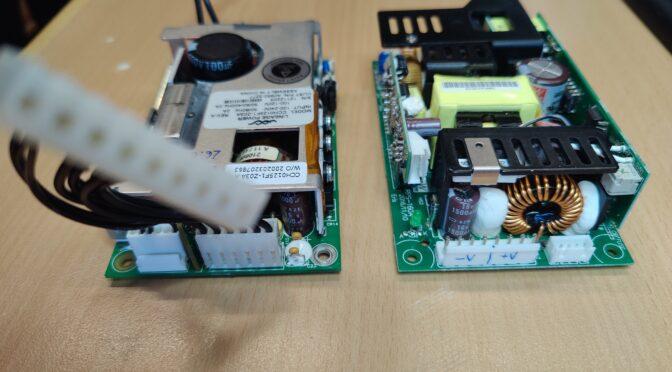
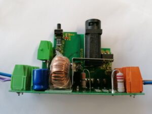
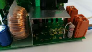
In the picture above: “new Meanwell Powersupply” below: “original Lineage Power”.

The power supplies are quite easy to repair, as described in the old report. However, the repair is also quite time-consuming. Of course, it is faster to install a new power supply. Unfortunately, the distributors of the Keysight oscilloscopes do not offer spare parts support and I could not find a direct supplier of the original Lineage power supply. But there is another alternative: In the forum of the EEV blog some users have found alternative power supplies that fit into the DSO-X oscilloscopes. A suitable model is the RPSG-160-12 from Meanwell. It is a 12V 160W power supply. The designation “G” in RPSG indicates that there is also a 5V standby supply. And it is exactly this function that the DSO-X needs. Because as described before, the front switch on the osci is not intended to disconnect the primary side of the mains supply, but only to switch a line on the DC low voltage connector to ground. This line controls the “PowerON pin” in the power supply.

Mechanically, the Meanwell almost fits on the mounting brackets of the DSO-X. “Almost” means that the distance between the mounting holes of the long side on the powersupply is about one millimeter further apart than the mounting bolts on the chassis of the oscilloscope. However, this can be quickly adjusted with a small round file or a 4mm drill bit. Now the Meanwell Powersupply can be attached to the oscilloscope chassis with the original Torx screws. The plug connection for the AC supply from the OSZI board to the power supply can be taken directly from the old power supply.

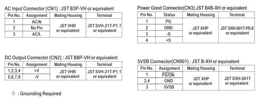
Pinout of the Meanwell connector strips

The 12V voltage supply at CN2 of the power supply is connected to pins 1,2,3,4 (+12V) and 5,6,7,8 (GND). The connection line to the oscillator must be adapted accordingly.

DC12V outputs on CN2

The picture below shows the pins of the connector strip on the oscilloscope labeled.

DC12V input to oscilloscope

I re-pinned the wires to fit and connected the connector to the powersupply as shown below.

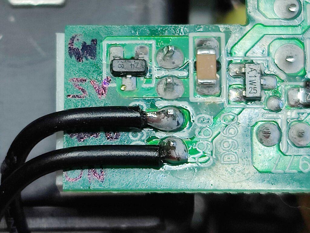
The main power supply to the oscilloscope is now established. Only the “power-on line” (PowerOn) is missing. For this I disconnected the 7th pin (GND) and the 9th pin (Switch) from the old connector and soldered them directly to the standby board of the power supply. The wire at the lowest pin of the standby board is the signal “PowerOn” and the one above is GND. So the power supply can be powered up with the front power switch on the oscilloscope.

“Control lines” for the PowerOn of the power supply unit


General view of the wiring

After a short function test and checking of the voltage (can be corrected if necessary also at the trim potentiometer at the power supply) the rebuilding is finished and the assembly can take place again.

Neumann KH-120 mystery noise fix

Loading

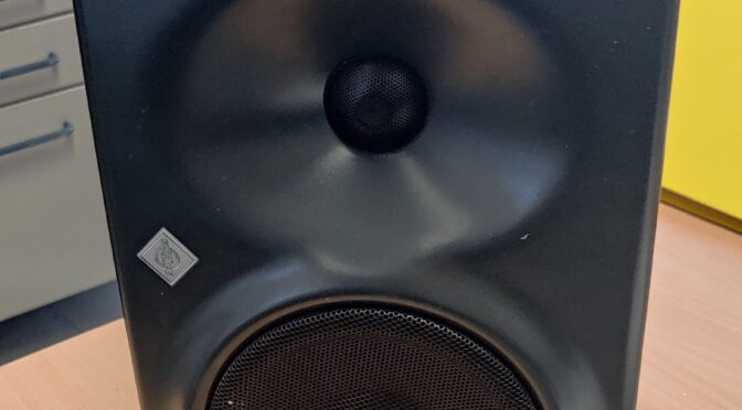
This time, a defective pair of active speakers found me, which comes from the professional corner of sound generating devices. These devices also occasionally have problems or fail. If you do a little research in the forums on the Internet, the KH-120 boxes are very robust and durable. The only issues I’ve read about are power supply failures. Occasionally there are also reports of a clear noise or whistling even if no signal is applied.

Exactly this problem was shown by these devices. After switching on, there was a hissing noise up to slight whistling tones. These could be influenced with the filter and gain switches, but not remedied. If the loudspeakers were in use for a long time – after about half an hour, then the noise decreased.
Unfortunately I didn’t manage to find useful information about these errors on the net, let alone a circuit diagram of the board. So there is nothing left but to search for it yourself, analyze the board and search systematically for the error.
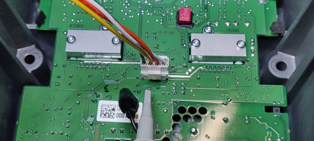
Starting with the removal of the four long Allen screws, the two halves of the housing can be carefully pulled apart. This then reveals two white blocks of insulation. These can easily be removed. The wire connection to the loudspeakers can be detached from the circuit board using a four-pole plug. Likewise the connection to the small LED logo board.

KH-120 is open and the insulation material removed
The picture shows the connector with the wires to the speakers

Next, the circuit board can be unscrewed from the housing. (a Torx bit is to be used here) All screws except for the two black cross-head screws must be loosened. Then carefully remove the board from the housing.

Circuit board of th Neumann KH-120

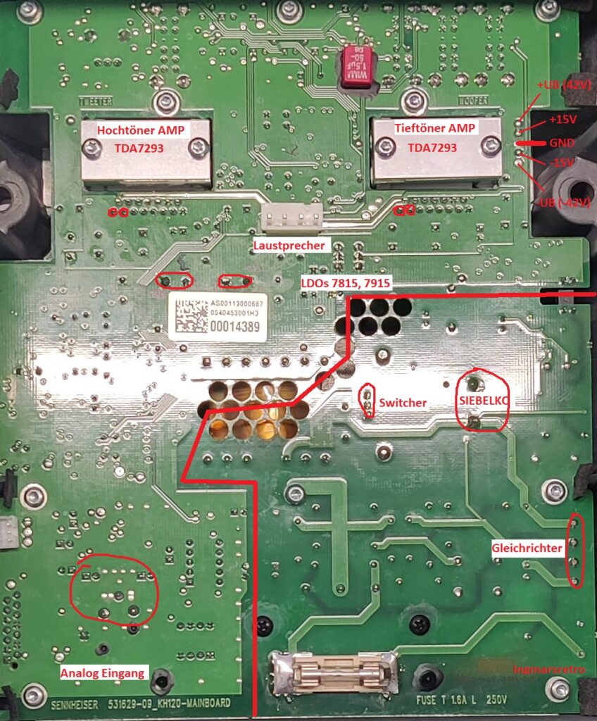
The board looks very good. All components that can be set into mechanical vibrations and possibly resonance by the sound are secured with elastic adhesive. The board layout is nice and clear. You can see the mains input and the mains filter at the bottom left of the picture. Above it is the large electrolytic capacitor for smoothing the direct voltage generated from the mains voltage.

The power supply is a switching power supply. The Mosfet controlled by a controller chip clocks the transformer. On the secondary side it is rectified again and the symmetrical voltages +Ub and -Ub for the power section of the output stages, as well as +15V and -15V for the supply of the pre-amplification and signal processing are generated. Ub is at -42 or + 42V. The power output stages are two TDA7293 ICs. One controls the tweeter and the other controls the woofer.

backside of the circuit board

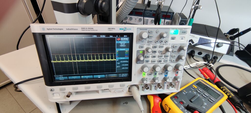
In order to look for the cause of the problem, one proceeds systematically. I first checked the supply voltages with a multimeter. Of course they are there. But you only see the truth when you look at it a little more closely. The multimeter is no longer sufficient here. An oscilloscope also reveals the AC component or residual ripple.

The picture shows the AC part of the -15V power supply. At around 800mV, however, it is suspiciously high. The period duration of these peaks with 30µs indicates that the transformer is regulated when the power supply unit hardly has to deliver any power. The switching frequency of the transformer can be seen within the pulses. But what could still be seen and cannot be seen in the still image are lower-frequency, asymmetrical components with an equally high amplitude. Accordingly, there appears to be a problem with smoothing the stress. So I examined the structure of the -15V supply. And look, the +/- 15V are implemented with a series regulator. A 7815 controller is used for the + 15V and a 7915 controller in the TO220 housing for the -15V. In the Note application, capacitors to ground are specified for the IC at the input and output. And that’s exactly what I took a closer look at first. An electrolytic capacitor with 100µF / 35V and 105 ° is used at the input of the 7915. This capacitor had to go out to measure. Immediately after the removal, it seemed to me that the weight of the component was too light – it didn’t feel like anything. So get to the LCR bridge and lo and behold, the capacity was somewhere around 1.4µF.

the polluter

A new electrolytic capacitor was installed quickly and the renewed measurement of the voltages revealed a nice signal again. The AC share was now much lower and the irregular disturbances had disappeared. Only the switching of the transformer could still be seen. What was still noticeable, or no longer noticeable, were the noises from the loudspeakers – the noise was gone.

the cause was built in here


Sony Walkman WM-DD11

Loading

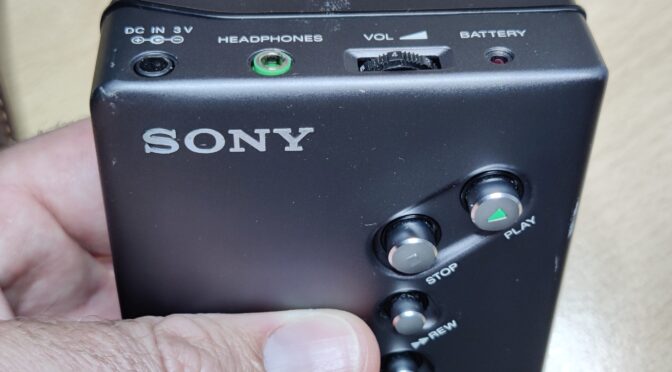
The portable cassette player from the manufacturer SONY with the type designation WM-DD11 is the content of this article. Colloquially known as “Walkman”, I received this part for my collection. Of course with the comment “defective” – ​​so again a little challenge and at the same time the hope that no mechanical, no longer available parts are affected. My request before the purchase whether there was any damage to the circuit board was also answered in the negative. The device is so far in order, the tape of an inserted cassette is moving – there is just no sound from the headphones. So ideal conditions for a restoration.

But unfortunately you cannot trust every statement and you cannot look “under the hood” beforehand and convince yourself whether the actual condition of a device corresponds to the description. When I held the part in my hands, the first impression was also very convincing. There were no noticeable scratches and dents. The area of ​​the battery compartment that was visible from the outside was also clean. So batteries inserted, also an audio cassette and then pressed on play. Lo and behold, the tape transport runs as described. Even as described, the part does not make any sound. So perfect starting conditions for my mini repair / restoration project.

But before I start dismantling, I did a little research on the history of SONY’s DD Walkman series. The first model in the DD series was sold in 1982. The designation “DD” stands for “Disc Drive”, which means that the “Disk”, i.e. the flywheel disk, is also part of the capstan drive system (motor). The belt for the other drives (tape reels) is placed directly around the disk. There are / were two price brackets of the DD models – the DD series with one-digit numbering (DD-1, DD-2, etc.) and those with two-digit numbering (DD-11, …). The devices with the single-digit number belong to the “high-end rail”. The device restored here comes from the “cheap line”. The DD-11 is not so high-quality and is also more simply constructed, but defective devices are available for very little money and are also fairly easy to repair. (The DD-11, for example, does not have a center wheel, an often defective part of the high-end series that is broken due to weak material. What then usually remains are defects in the electronics or on the mechanical side – an aged belt The belt is the same as that already installed in the legendary TPS-L2 Walkman and has the component serial number: SN 3-499-042-99 (this source or number has not been verified) You can also find the belt if you go to “TPS -L2 belt “searches on various online portals.But now enough information on the general part. I experienced a sobering and grounding of my restoration euphoria immediately after unscrewing and opening the case. Unfortunately, the circuit board is not at all undamaged. Once again someone did not remove the 1.5Volt cells and left them in the device for a very, very long time.

The batteries that leaked, as it is, have left clear marks on the circuit board. This means that extensive cleaning of the circuit board is necessary before the search for corroded conductor tracks can begin.

After cleaning and removing the battery electrolyte residues, I was able to make out a few defective conductor tracks. Fortunately, these are pretty easy to fix. In most cases it is sufficient to remove the solder resist in the defective area and to tin the exposed copper tracks. Depending on the width of the track, the defective part of the track is then reconnected with individual strands or wires.

Now the time has come to carry out a first functional test after a provisional assembly. And as described, the capstan drive works, the tape is transported – but there is no noise whatsoever from the connected speakers. Now is the time to look at the number one source of failure – the old electrolytic capacitors. Eleven of these are installed on the board.

When I removed the first electrolytic capacitor for a capacity test, the well-known fishy smell rose again. As expected, the capacitance of the capacitor was also well below the nominal value. So I made a spontaneous decision to remove all eleven electrolytic capacitors in order to swap space. (In modern language it is called “recap”: D)

The following values ​​must be renewed:
– 5 Stück 220 µF / 4V
– 1 Stück 100µF / 4V
– 3 Stück  47µF / 4V
– 1 Stück 10µF / 16V
– 1 Stück 4.7µF / 25V


I like to replace the SMD electrolytic capacitors with SMD multilayer capacitors, as these are now also available in very small designs in high capacities with suitable dielectric strength.

After the renewal, the board looks nice again. A repeated provisional commissioning shows that the effort was worth it. The music on the inserted tape sounds in the expected quality. The next step is to calibrate or adjust the belt speed. A reference tape is required for this. Years ago I recorded one with a very good tape recorder. The recording consists of a 1kHz and a 5kHz sine tone. This band is now used as a reference in the DD11. To do this, the output of the DD11 is connected to a frequency counter or oscilloscope and adjusted with the trimmer potentiometer during playback until the 1000 Hz or 5000 Hz can be seen exactly on the oscilloscope.

The Walkman can now be reassembled. All screws are properly tightened again and finally the function tested again and the beautiful piece can be put in the showcase …

HomeMatic smoke detector HM-SEC-SD quick repair

Loading

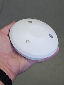
This time again a quick article on the subject of “Aging and Homematic Smart Home”. It’s about the following device: The Homematic smoke detector HM-SEC-SD, i.e. the older version of the smoke detector from eq3.

First of all: This article only shows how I put this device back into operation. Since it is a safety-relevant device, an acceptance test by a certified testing company would have to take place after the repair in order to be allowed to continue using it. So the contribution only provides what has become broken in the device.

So what is it about? The radio smoke detector HM-SEC-SD showed the following symptom during the monthly test (yes, you should press the test button once a month):

A short press on the button and there was no acoustic signal – instead the red signal LED flashes several times at approx. 0.5s intervals. Replacing the batteries does not change anything, the behavior remains the same. The radio module of the detector behaves normally. It can be reset and taught again. In this case, a look at the operating instructions (under point 9.2 on page 24)

– If only the LED starts to flash after pressing the button, the smoke detector is defective and must be replaced
So time to open the detector and take a look. My first suspicion fell on the detector chamber and that there is contamination here or that an animal has settled in the chamber …
Smoke detector opened

But after removing the lid of the detector chamber, no animal intruders were to be found. However, a strange pattern could be seen on the inside of the lid:

Streaks on the inside of the detector cover

These streaks, I thought at first, were created during the injection molding of the plastic component and must be like that. But on closer inspection and a “wipe” with your finger, they could be removed. In short, these streaks are dust particles. And when they are on the lid, then also in the entire measuring chamber. So blow it out with compressed air, put the cover back on and test it. -> same mistake as before. So again, put the lid down and take a closer look with a magnifying glass. The coarser dust, if you can speak of “rough”, was gone, but the surface of the photodiodes still had very fine and difficult to see streaks. So I cleaned the chamber and the diodes with a little alcohol on a cotton swab.

thorough cleaning required

Another function test showed success – better partial success. After pressing the test button, the piezo squeaked – but only very, very quietly – and by that I mean barely audible and the LED flashed nine times at an interval of one second. So actually the way it should be. Just way too quiet. So something had to be broken. So I examined the circuit starting with the piezo and quickly found what I was looking for. The piezo is controlled by a 40106, a 6-fold Schmitt trigger. In order to get enough electricity, three “Schmitts” are connected in parallel. The output was low-resistance, which is actually not allowed to be. So unsoldered the 40106 and measured it again. Between pin 1, 2 and 7 (input and output of the first Schmitt trigger and the VSS pin) there was a full short circuit. That means the IC is defective.

6times Schmitt trigger IC 40106

After the IC was exchanged, the smoke detector could finally “scream” again as usual.

Homematic actuator quick repair (dimming actuator RS485)

Loading

I have another small contribution to make on the subject of “Aging and Homematic Smart Home”. Many thanks to Fritz for the preparation and analysis.

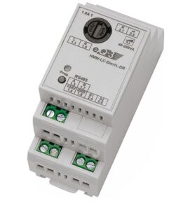
As in the last post “Homematic actuator quick repair”, this time it is again about a device from the Smart Home series. It is the dimmer actuator with the designation “HMW-LC-Dim1L-DR”. This is a phase control dimmer actuator for incandescent lamps and low-voltage halogen lamps with conventional transformers. Many modern LED lamps can also be controlled with this dimmer. The actuator belongs to the “wired” series, which means that it is not connected to the CCU via the BidCos radio protocol, but via the RS485 bus. The actuator receives the power supply for data communication from a 24V power supply unit. This also supplies the µC in the actuator. The network side is supplied with control data from the low-voltage side via an optocoupler. This ensures galvanic isolation. On the network side there is a dimmer controller module, which in turn controls the triac. This controller must be supplied with a voltage of approx. 15V. To generate this, the manufacturer has built in a capacitive voltage divider. And this is where the aging problems begin …

The error pattern manifests itself as follows: The connected light source cannot be dimmed or switched on. However, the dimmer is communicating correctly with the bus. The red function LED lights up correctly. The commands for “Off” and “On” via buttons are also displayed in the CCU.

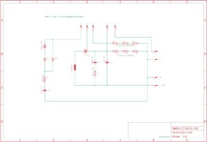
Circuit diagram of the mains side on the “main board”
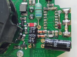
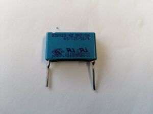
defective 330nF X2 capacitor

The cause: According to the data sheet, the IC U2008, a dimmer control module, is supplied with a voltage of DC 15V. In this case, the supply voltage was significantly lower (at approx. 5.8V). This supply voltage is made the 330nF / 275V X2 capacitor C4. The capacitor is optically in perfect condition, but a simple capacitance measurement quickly shows that nothing fits here. The capacitor C4 only had a capacity of approx. 30-40nF. So it’s like so often -> It was the capacitor: D

Dimmer module side view

After the replacement, the voltage on the U2008 was ok again and the dimmer is doing its job again. As a preventive measure, the two other X2 capacitors on the board (C1 47nF / 275V and C2 100nF / 275) were replaced.

Installation locations of C1 and C2


Wall socket with integrated USB port (repair)

Loading

Thanks to the USB standard, it is now easy to operate or charge your mobile phones, tablets, Arduinos, Raspberry PIs, toothbrushes, power banks, etc., etc., with one and the same charging adapter or plug-in power supply. The “plug-in power supply” is an AC / DC converter which, ideally, electrically isolates the mains side with the 240VAC / 50Hz from the low-voltage direct voltage side in compliance with the applicable regulations. The low-voltage side provides the 5VDC via a USB-A socket. Depending on the model and origin, maximum currents of 1A up to approx. 2A can be taken.

Due to the large number of USB-powered devices in households, there are also quite a few of these plug-in power supplies. In order to operate the plug-in power supply, you naturally also need a socket in the house installation in order to connect the power supply to the utility grid. If several USB devices are in operation, or better – in charging mode, some of the sockets in the household are quickly occupied and the power supply for more important devices such as coffee machines and the like is missing …

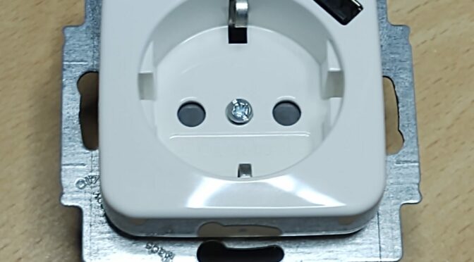
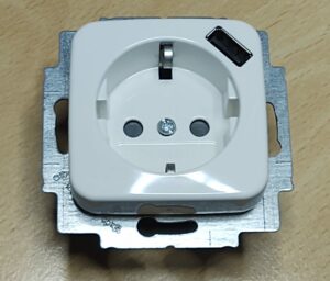
Some manufacturers came up with the idea of ​​integrating a USB-compliant power supply unit with a corresponding USB socket into a Schuko socket that was designed for installation in a wall outlet, without losing the space for the Schuko socket.

These sockets with integrated USB power supplies are nothing new and have therefore been on the market for several years. Of course, I also had to install such sockets at the time, because they are really extremely practical. So – now, of course, the years have passed and the service life of the power supplies built into the sockets is coming to an end and they will fail. More precisely, they no longer provide a 5V supply.

no more voltage at the 5V output

However, since I don’t throw everything away and replace it with new ones – the sockets were also expensive at the time – my plan was to look for the fault and repair them if possible. In this case it is a Busch-Jaeger socket of the type 20EUCBUSB-214-500 which now refuses to function. The power supply unit should require approx. 100mW in standby mode and with 5VCD it can deliver a maximum current of 700mA.

After removing the socket, it was also quickly dismantled. The plastic cover attached to the rear is held in place on the opposite side by means of locking lugs. Now a circuit board came out that can be easily pulled out. The contact to the network side and also to the USB socket is realized via spring contact pins. It should be mentioned right away – they fall out quickly. That is why you should always work the socket with the back facing up. This saves you the hassle of searching for the little pens.

cover removed
Socket without power supply board


When the board was now released from its housing, at least one problem was revealed, which explains the failure of the power supply. A small chip on the board had a hole that definitely doesn’t belong there. The components surrounding it also showed traces of smoke. Thanks to another functioning socket of this series, I was able to identify the IC.

Power supply board
the hole in the IC doesn’t belong there
“Gunsmoke traces” on the resistance


It is a Link Switch-II series LNK614DG from PowerIntegrations. It is a small ALL-IN-ONE IC that has integrated the power FET, the oscillator and the control via a feedback winding of the transformer. The power rating according to the data sheet is 3.5W installed in a closed housing and 4.1W in an open frame or ventilated state.

“typical” application – Quelle: Datenblatt https://ac-dc.power.com/products/product-archive/linkswitch-ii/

The chip therefore only needs a few peripheral components, which in this case also makes it easier to search for further errors. On the network side, only the AC rectification and smoothing as well as the line filtering are necessary. These components were in top condition and worked. Then there is only the transformer with its primary, secondary and feedback winding, the secondary rectification and smoothing and a few resistors that are connected as a divider. No fault was found with any of these components. So – who dares wins – the IC ordered and exchanged – and bingo – the 5V are back at the exit and can also be loaded.

the new chip before installation 🙂


Tomy Racing Cockpit – electrical wiring

Loading

Due to some inquiries regarding the electrical wiring of the Tomy Racing cockpit, I sat down and drew out the wiring. There are apparently many contemporaries who still find toys from the 80s in their basements, attics, etc. and repair them again. With the Tomy Cockpit it happens again and again that the thin wires break off when they are dismantled or the soldered joints no longer hold, often forgotten cells in the battery compartment have dissolved and the contacts and soldered joints are corroded as a result.

I show a sketch of the wiring in the following figure.

By the way, I only use two 1.5V cells, since the parallel connection of two cells each in the battery compartment is nonsense, as the cells are guaranteed to have different internal resistances and thus comfortably discharge each other even when they are not used.

In order to be able to identify the components shown in the sketch in the racing cockpit, I also took photos of them.

This is the back of the “switch” that represents the cockpit’s ignition lock and with which the system is switched on.

I called this part “breaker” because it is a normally closed contact that is triggered by a small “gearwheel” and causes the drum lighting to flash. That happens when you leave the “street”.

These are the connections of the battery box. I doubt whether the colors of the wires are the same for all versions. Because in the devices that I have since revived, different wire colors were installed.

With this information it should now be a little easier to recreate the broken wires and solder joints.


USB stick defective?

Loading


Again and again it happens to me that a USB memory stick loses its function and is suddenly no longer recognized. Often the stick is still registered as a drive in the system, but it lacks the disk, or even the system reports that the stick is not formatted. And even though he just recently, full of important data, has worked in another computer. 🙂 (Here would now be the story with the backups or backup copies …). All these problems are mostly due to operator errors or mechanical problems. For example, an operator error may be that the stick is being pulled while one more writing is in progress. The stick is then de-energized during a process. And depending on whether the controller or flash memory can handle it, the stick will survive or not. Often, mechanical defects are the cause of breakdowns. So it may be that the solder joints between the connector and the board break, or get the connecting pins of the quartz or oscillators contact problems.

In this case, I got a miniature stick from extrememory, which does not want to give away its stored data. It is displayed in the system administration, but if you want to access it, the message “no data carrier found” comes. The attempt to format or partition over diskpart from the commandline did not work. Also various tools like “SDFormatter” or “USBstick_Formattool” failed. Even with Linux or on MAC systems, no success was achieved. So a stick for the barrel … But I thought, even if the stick in its small design rather not close to a mechanical defect – why not take a look anyway 🙂 And at 16GB I will not give up so fast.

So I tried to gently open the case by first removing the metal case of the USB connector.

That works quite well. After I wanted to take a closer look at the appearing small printed circuit board with its tracks, there suddenly appeared something familiar.

That looks like an SD card. More specifically, like a microSD card.

That’s the way it was. The USB stick is nothing more than a MicroSD card reader, in which such a card is installed. Using tweezers, the SD card could be levered out.

Apparently here again the problem is with the contacts, or contact springs between card and card reader. It is the cause of the problem, because the SD card worked fine in another card reader and all the data was available. It pays to invest in front of the garbage bin for a few minutes and to inspect the innards of the device.

Sony RX100 digital camera (and its repair)

Loading

The Sony RX100 digital still camera with its 20.2 megapixel EXMOR CMOS sensor impresses with its excellent image quality and compact design. The sensor size of one inch and the front Zeiss Vario Sonnar F1.8 lens are also responsible for the good image results. With 10x6cm and a thickness of 3.6cm, the camera is still suitable for pockets. (Although I would not recommend it). The 3.6x optical zoom lens is retracted when it is switched off and extended when in use.

But after some time and a number of in´s and outs of the optics, it may – or better – it will come to a situation where the optics refuse to serve. This manifests itself in different ways. Either nothing happens after switching on, the optics do not move and only the message (“Power Off and on again”) appears on the display, or the lens moves out a bit and then back in again. Now you could assume that the camera has mechanical damage, the sliding surfaces inside the optics are dirty, or something is bent or warped and jammed by a possible fall. But that’s usually not the case. In this case, the camera has never been subjected to strong mechanical, thermal, etc. stresses and there is still an error. If you do a little research on the Internet, you will find some repair tutorials where you try to clean with some paper strips between the slide rings of the optics etc. No reasonable information was found. So I have no choice but to look for the cause of the problem myself. And it was found quickly. After opening the device and slightly lifting the rear housing cover, the object suddenly extended again. If the lid was replaced, the problem was there again. So there had to be a contact error somewhere. In the following lines I present my way to a functioning camera:

After loosening the screws and removing the plastic base plate, the rear cover can be removed with the control panel and the monitor.

The Flexprint for the screen and the one for the control unit can be released, the small speaker can simply be hung up. Now the battery can be inserted and the camera can be switched on again. In this case the lens opened and extended again correctly. So it’s really a contact problem. But where? I tried to put light pressure on the Flexiprint, which supplies the mechanical part of the optics. (Not the one that leads from the sensor to the mainboard.) With this slight pressure on the Flexprint, the device was switched on again and lo and behold -> hit. The optics didn’t move. That could also be understood. So this Flexprint seems to have a line break at the kinks. Apparently, this print is mechanically stressed due to the construction and retraction of the lens and thus yields and breaks at some point. (Perhaps also planned obsolescence). Anyway, I looked for a replacement on the net, found it and after a week of waiting the new Flexiprint was already delivered.

The new print for the optics is sold without any components. This means that from here a little experience in handling soldering tools, SMD components and flexible circuit boards is required.

The optics must be exposed and removed. To do this, the mainboard must be detached. (three screws in total). Then carefully remove the black film from the back of the optics. (Be careful with all flexible cables) Once the film is off, the flexprint to the sensor can be unplugged.

Next, the motor unit is released and the motor is separated from the lens housing.

There are some components on the print, such as plug connections and small fork light barriers, which are installed in the lens (lens position) and in the motor unit (two pieces as incremental encoders and for determining the direction of rotation). These are held in place with small metal brackets and must be released before removing the lens unit.

The lens, drive unit and mainboard are removed. All plug connections between the optics and the drive motor must be disconnected.

The motor unit can now be separated from the lens. The Flexiprint is attached to the lens housing with tape and small hooks. These have to be solved.

Now disassembly of the motor unit continues. As previously mentioned, there are two fork light barriers in the plastic housing of the motor gearbox, which are also held in place with a clamp. This can simply be clipped out. To complete the removal, the motor must be unsoldered. Now the Flexiprint is free and the delicate step can begin.

The small SMD connectors must be unsoldered from the old print and reattached to the new print. This work requires cleanest hand towels, as the small plastic housings can be easily destroyed when unsoldering. I recommend here to heat the print only from the bottom, and then lift the plug off with tweezers. Otherwise you run the risk of deforming the plastic of the connector too much heat. If this is successful, the plugs can be soldered onto the new Flexprint.

The same work is also to be done with the fork light barriers. Then only the contacts of the motor have to be soldered to the designated positions in the flex board.

If that worked, the assembly can be done in reverse order. When bending the flex board into the correct position, you can orient yourself on the old board. Then the installation should not be a problem. A function test should be carried out before attaching the rear wall of the camera (rear cover). The lens must extend and retract without a monitor or control panel. If that also works, then it can be finalized. In my case, the repair was successful. Let’s see how long it takes for another conductor to break in the flexible PCB …

IPhone 5s under the wirebonder

Loading

IMAG1839
IPhone 5S the maginfier glass 🙂

If the screen of an IPhone 5S gives up its ghost once (that is, it breaks or something similar), then the only thing that helps is swapping it. But beware ! The screws that hold the shield plate over the three Flexiprint connectors from the display are NOT the same length.

There are screws of different lengths here – even if you don’t necessarily recognize it optically. If you don’t take great care to screw all the screws back into the original threaded bushing during assembly, then it has already happened. The screws, which are approx. 0.1mm long, protrude over the socket and touch and damage the surface of the circuit board. If someone then takes it very carefully and tightens the screws firmly enough, then these are pressed into the second layer of the board. And that’s exactly where seven parallel conductor tracks run, which together require a width of almost 1000um (1mm). Now you can imagine what the tip of a screw can do here.

Exactly – chaos and destruction. The almost 50um wide conductor tracks have no chance against the colossus of screw with 1000um.

The result: Several of these conductor tracks are cut and the mobile phone cannot find all of its electronic components after switching on and starts the boot process again cyclically (with a brief flash of a blue screen)

Usually the device is now ready for the bin, or at least a new mainboard would be required. Just such a cell phone recently landed on my table.

IMAG1829_1
figure 1

The connections to the display can be seen in Figure 1. At the bottom right, at the black spot, was the threaded socket into which the screw that was too long was screwed. If you now remove the socket, you can examine the damage.


The enlargement in Figure 2 shows clear impressions of the screw and a slight copper shimmer can also be seen.

However, the extent of the damage can only be determined if the layer is exposed in the area. With a suitable microscalpel I tried to expose the plane.

IMAG1827_1
figure 2
IMAG1831
figure 3

Figure 3 shows the conductor tracks and their interruptions. A repair with a soldering iron and repair wire is no longer possible here.


figure 4

But since I have the opportunity to work on a wirebonder, I had the idea to use it for a repair attempt. The bonder from TPT-Wirebond offers the functions of wedge and ball bonding in different wire diameters. I could imagine wedgebonding as a suitable and feasible variant. The 25um diameter bond wire should fit. Only for the problem with the temperature of the chuck I had no solution. Because it is certainly not a good idea to heat up the iPhone. So I tried to bond cold. Without further ado, the chuck was disconnected from its power supply, the ultrasonic energy of the bonding tool increased and an attempt was started. Lo and behold, the bond holds. So, without further ado, six of the seven lines were made conductive again with gold wire bridges (Fig. 4) and then the display was connected for a start attempt. Lo and behold, the iPhone started normally again.


IMAG1837_1
figure 5

Now it was only a matter of protecting the sensitive bond wires from damage.

Here a synthetic resin two-component adhesive offered itself, from which I mixed an amount the size of a pin and covered the repair area with this droplet. After hardening, I was able to put the phone back together (at the repair site, of course, without a screw. A short function test was positive.;)