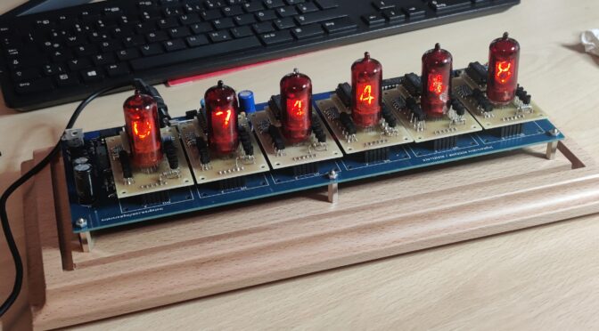
Tag Archives: Atmega328

Selfmade Nixiclock

Loading

The fact that the topic of retro has become more and more of a trend in recent years has not escaped me either. The “Industrial” and “Steam” style has also found its way into many households. People put many things on the shelf again, which represent the robust technology and the appearance of the past decades. For example, LED lamps flicker in the rooms, which were visually modelled on the light bulbs of the Wilhelminian era. The brass lamp holders are held in place by a cable sheathed with fabric mesh. Instead of the carbon or tungsten filaments in the bulbs, modern LED filament works. Thematically corresponding to this style, mechanical watches and electric clocks with illuminated displays of all kinds, for example, are in demand again. In keeping with this trend, I have already reported on the VFD watches in older blog posts. (VFD = VaccumFLuoreszenzDisplay) Until the end of the 90s, for example, this display technology was still frequently used in video recorders, hi-fi devices and various radio alarm clocks. After that, LED and LCD technology was standard. Today, the small OLEDs are finding their way everywhere. As part of the Retro Revival, VFDs are assembled into watches in the form of single-digit display tubes. These watches are available as finished devices or as kits (grother.de). Since these display tubes are no longer manufactured and only old stocks (new old stock) are available, prices are also rising. But it is even worse in terms of price – a technical development from the 1920s is a display technology based on the principle of the glow lamp. In this case, in a glass flask filled with noble gas, a digit bent from wire is attached as a cathode, in front of a thin metal grid as an anode. If a voltage is applied, the noble gas begins to glow along the wire formed as a digit. Seen from the outside, this creates the impression of a luminous number. In such a tube, the digits from 0-9 are usually accommodated and for each digit there is of course a separate connection. Many of the readers will surely know this type of tube. It is called NIXIE – display tube (comes from the designation “Numeric Indicator eXperimental No. 1”

A watch with such display tubes is still missing in my collection. So I wanted to own one. But buying is easy – and also very expensive. So I decided to build a Nixie clock myself. It all started with a lengthy search for the tubes, because even for these you have to lay down a lot in the meantime. And I need at least six pieces, because my watch should also have a second display. So I searched the Internet on various platforms – and in the bay I found what I was looking for. There a board equipped with Nixie tubes was offered, which was broken out of some old device. The function of the board was given as “unknown” – but it was very cheap. The seller had two of them. So I risked it and bought the two boards equipped with five Nixies each.

The tubes were then successfully soldered out with some caution. The type of tube is the Z574M, for which you can also find the data sheets in the network and thus also has the socket circuitry.

With the help of the wiring, it can then be easily contacted and thus check digit by digit of each tube. The characteristics of the 574 are:

  • Anode ignition voltage: 150V
  • Anode burning voltage: 140V
  • Anode extinguishing voltage: 120V
  • Max anode voltage: 170V
  • Cathode current min: 1.5mA
  • Cathode current max: 2.5mA

With a suitable power supply unit, I was able to quickly set the necessary supply voltages for the functional test.

You can see here that the tube draws a current of 2.8mA at a burning voltage of just under 140V. This corresponds to an output of 392mW. So if I extrapolate and all six digits of the watch are continuously energized, then the power supply for the tubes must bring about 2.3W.

So the tubes already work. Now I can think about what the clock should look like and even more how I want to design it.

The idea is that a microcontroller should control all six tubes. I want to realize this with 8-bit 4094 shift registers, of which four bits each are used for a tube. These four bits from the shift register should then control the tubes via binary coded decimals (i.e. BCD). However, since the tubes have a connection for each digit, ten separate digit controls must be generated from the four BCD lines. This will be done by a CD4028. The IC CD4028 is a “BCD to Decimal Decoder”. To switch the relatively high voltages of the Nixies, the BCD decimal decoder will drive a suitable transistor. This is where the MPSA42 will do its job. This is an NPN bipolar transistor with a collector-emitter dielectric strength of 300VDC at a maximum collector current of 500mA. In order to be able to use the tubes as flexibly as possible, I have come up with the idea of designing a separate circuit board for each tube. These individual display boards should then be plugged into a main patine. So if a digit is defective, you can simply pull out the board in question and repair it. Then you don’t have to solder around the motherboard.

The microcontroller should find space on the motherboard. The low- and high-voltage supply and the shift registers are also to be accommodated on the mainboard. The display boards only carry the Nixie tube and its driver transistors and the BCD decimal decoder. By means of post connectors, they should be easy to plug into the motherboard. To make these formulations a little easier, I have made this sketch:

Based on this idea, I now began to draw the circuit diagrams. So it started with the display board on which the tube is located. The circuit design is very simple. Two opposite post connectors should give the board a stable hold on the motherboard. One of the connectors supplies the BCD decimal decoder (CD4028N) with the four data inputs and the 5V supply voltage for the logic. On the other side of the board, the “high voltage” is provided for the tube.

From this I could then simply create a layout and then produce it as a prototype as a board.

Nach dem Ätzen und Bestücken der ersten Platine und fünf Weiteren war der erste Schritt der Nixieuhr getan:

In order to test the first part of the work, I had a DEB100 digital experiment board available at my workplace. The following short video shows the test result:

After all six boards were equipped and tested, I had dealt with the planning of the motherboard. At the beginning, of course, there was again the creation of a circuit diagram. From an external 12VDC source, which should ideally be a simple plug-in power supply, the supply voltages had to be generated. On the one hand I needed a 5VDC supply for the microcontroller, the shift registers and the BCD decoders and on the other hand a “high voltage” of 140VDC for the Nixie tubes. The 5V supply was done quickly – here a 7805 linear controller should do its job. Since the power consumption of the digital components is relatively low, no complex measures were required here. The 7V difference on the 7805 at the few milliamperes he packed without great power dissipation heat dissipation. For the generation of the 140V I made a step-up converter with an MC34062 (Inverting Regulator – Buck, Boost, Switching) controller, which switches a 220uH inductor via a FET. Via a voltage divider with trimming potentiometer at the output, a voltage feedback can be sent to the comparator output of the controller and thus the output voltage can be adjusted. As a microcontroller, I always use Atmega328 and the like for most of my projects (due to the stock level :)). This is also the case here. The result is the following circuit diagram:

From this I made a layout again and etched and equipped a board again. However, this prototype test board was only a version with four digits. The reason was also that I did not have a larger raw board available 🙂

From this I made a layout again and etched and equipped a board again. However, this prototype test board was only a version with four digits. The reason was also that I did not have a larger raw board available 🙂

After various successful tests with the prototype board, I ordered professionally manufactured boards from the board manufacturer I trust. After assembling them, I then created a test program that could control all digits. A short test video is linked below:

The following photos show how the clock looks with the “beautifully” manufactured boards. To make the whole work even more nostalgic, I had the idea to mount the boards on a milled wooden panel. (Thanks to Gebhard for the woodwork). In order to keep the watch electronics permanently dust-free, I had a transparent Plexiglas hood made.

Sketch for the arcyl glass hood

As so often, I made the software with the Arduino IDE. To flash the microcontroller I use the AVRISP mkII Programmer. If somebody is interested in the code, I can also post it here on the blog.


The Wetterfrosch 2.0 or environmental data logger

Loading

A few years ago I presented a project in which a Raspberry Pi was working as a data logger. A few sensors were connected to this Raspberry, which recorded environmental data such as air temperature, relative humidity, air pressure and the current GPS position. The sensors mostly consisted of ready-made breakout boards that were connected to the RaspberryPi via the various buses (I²C, Serial, SPI …). Python scripts ran on the PI itself, which read out the sensors, summarized the data and stored it on a USB flash memory. I then built this hodgepodge of components into a plastic box with a size of 150x80x50mm.

But it’s also about a lot smaller. As part of a small project, the task was to downsize this sensor / data logger. My approach to realizing this was very simple: “Everything new”. So I changed the concept like this:

  • the RaspberryPi is replaced by a microcontroller
  • a circuit board is created on which all components are housed
  • the recorded data is saved on a microSD card
  • the board is reduced to the most essential components. The sensor electronics and the SD card reader are placed directly on the board
  • a GPS receiver (in the form of a breakout board) should be able to be plugged in as an option
  • the controller is programmed via an ISP interface
  • the power supply is 5V DC

From this I created the following block diagram:

Block diagram

As is so often the case, the central element is the Atmega328 microcontroller. As an external circuit, it only needs a quartz for clock stabilization. (More precisely, it also offers the option of using internal oscillators …) The microcontroller communicates with the sensors HYT939 and BME280 via the I²C bus. The level from 5V on the controller side to 3.3V on the sensor side is adjusted via the sophisticated bidirectional level shifter circuit using a BSS138 Mosfet with an integrated body diode. This circuit is used for both the SCL (Serial Clock) and the SDA (Serial Data) line.

The data is saved on a microSD card. A card slot is installed for this, which communicates with the controller via SPI (Serial Peripheral Interface). An adjustment of the signal amplitudes is also necessary here. This time, however, the TXB0108 chip from Texas Instruments takes care of that. This is an 8-bit bidirectional level shifter.

A button will start and stop data recording and a LED will display various status messages through flashing sequences.

The optional plug-in GPS module works with a 5V power supply and the levels of the serial data communication (RS232) are also 5V compatible.

Last but not least, the power supply must of course also be planned. Only an external, stabilized 5VDC source should be connected here to supply the logger. The 3.3VDC required for the sensors and SD card are generated on the board by means of an LDO (Low Drop Out) controller.

Once all components and their interaction have been defined, the circuit diagram is drawn from them. For my handicraft projects I mainly use the schematic and layout editor “eagle”. The circuit shown below results from the block diagram.

From the circuit diagram I created a layout with two layers, the floor plan of which has the dimensions 55x25mm. Except for the connectors, only SMD components are on the board.

In the layout tool there is the function to view an optical preview of the finished board. In this way you can check in advance whether the board corresponds to the requirements and, if necessary, optimize the position of the components. Once this is done, a package with production files (Gerber files) is generated from the design and this is then sent to the circuit board manufacturer you trust. Since it is also located very, very far away, production also takes a few days. But in the end the circuit boards arrive and are also impressive. 🙂

The two pictures above show the board from the TOP and the BOTTOM side. The next step is to order the components according to the plan and then assemble them.

I do the assembly by hand with a soldering iron suitable for the SMD components with a correspondingly small tip. For the very small parts, such as the BME280 sensor, a microscope or microscope camera is also used.

The two pictures above show what the board looks like after it has been assembled. The following photo shows the size difference of the finished logger with the attached GPS module compared to the old “weather frog”After completing the hardware, it is now time to start with the software. I tinkered it in a practical way with the Arduino IDE tool and flashed it to the controller via AVRISP mk2 via ISP. In order to get the AVRISP to work on a Windows 10 computer, a suitable driver must be installed. (libusb-win32-1.2.6.0 helps here)

program code created with the ArduinoIDE
controller flashed with AVRISPmkII

Data recording is started on the SD card after applying the supply voltage and pressing the button. The measured values ​​are written every second. If, as in this example, the GPS sensor is plugged in, the GPS data is also recorded. The software also records if the GPS sensor does not have a “fix” yet. (Since there was no GPS fix in the example log below, no valid GPS data is included.)

Example of the data log:

Luftdruck962.41
Luftfeuchte37.05
Temperatur26.96
-----------------------------
$PGACK,103*40
$PGACK,105*46
$PMTK011,MTKGPS*08
$PMTK010,001*$GPGGA,235947.799,,,,,0,00,,,M,,M,,*71
$GPGLL,,,,,235947.799,V,N*73
$GPGSA,A,1,,,,,,,,,,,,,,,*1E
$GPGSV,1,1,00*79
$GPRMC,235947.799,V,,,,,0.00,0.00,050180,,,N*48
$GPVTG,0.00,T,,M,0.00,N,0.00,K,N*32
$GPGGA,235948.799,,,,,0,00,,,M,,M

-----------------------------
Luftdruck962.39
Luftfeuchte36.72
Temperatur26.95
-----------------------------
Luftdruck962.43
Luftfeuchte36.66
Temperatur26.97
-----------------------------