Thanks to the USB standard, it is now easy to operate or charge your mobile phones, tablets, Arduinos, Raspberry PIs, toothbrushes, power banks, etc., etc., with one and the same charging adapter or plug-in power supply. The “plug-in power supply” is an AC / DC converter which, ideally, electrically isolates the mains side with the 240VAC / 50Hz from the low-voltage direct voltage side in compliance with the applicable regulations. The low-voltage side provides the 5VDC via a USB-A socket. Depending on the model and origin, maximum currents of 1A up to approx. 2A can be taken.
Due to the large number of USB-powered devices in households, there are also quite a few of these plug-in power supplies. In order to operate the plug-in power supply, you naturally also need a socket in the house installation in order to connect the power supply to the utility grid. If several USB devices are in operation, or better – in charging mode, some of the sockets in the household are quickly occupied and the power supply for more important devices such as coffee machines and the like is missing …
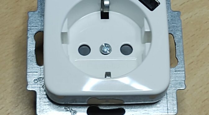
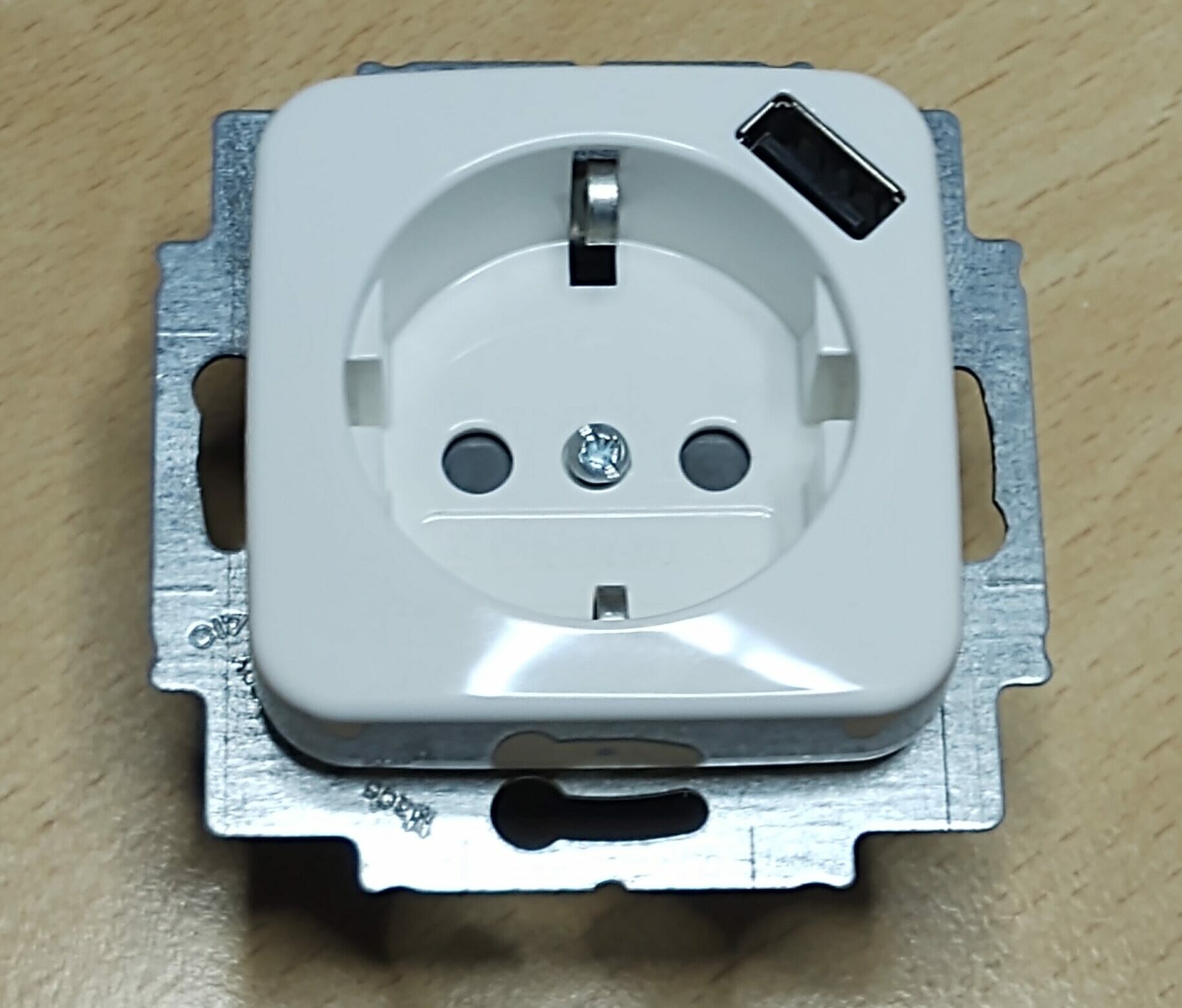
Some manufacturers came up with the idea of integrating a USB-compliant power supply unit with a corresponding USB socket into a Schuko socket that was designed for installation in a wall outlet, without losing the space for the Schuko socket.
These sockets with integrated USB power supplies are nothing new and have therefore been on the market for several years. Of course, I also had to install such sockets at the time, because they are really extremely practical. So – now, of course, the years have passed and the service life of the power supplies built into the sockets is coming to an end and they will fail. More precisely, they no longer provide a 5V supply.
no more voltage at the 5V output
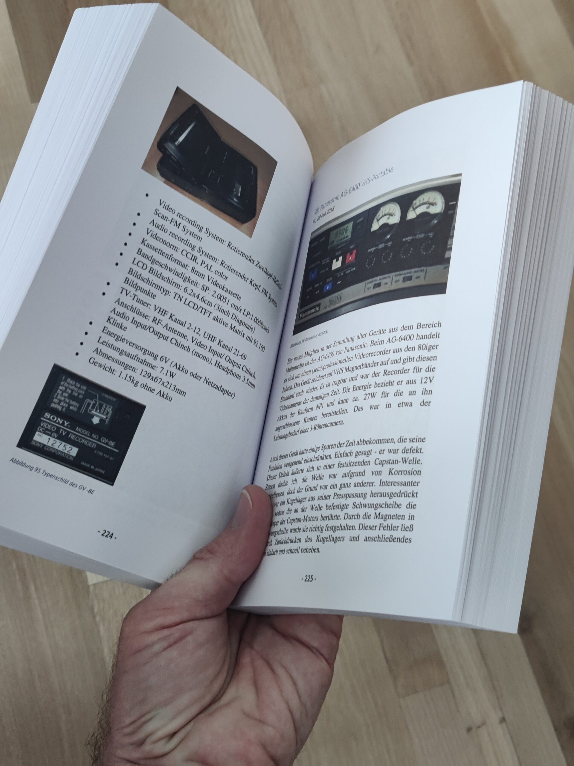
However, since I don’t throw everything away and replace it with new ones – the sockets were also expensive at the time – my plan was to look for the fault and repair them if possible. In this case it is a Busch-Jaeger socket of the type 20EUCBUSB-214-500 which now refuses to function. The power supply unit should require approx. 100mW in standby mode and with 5VCD it can deliver a maximum current of 700mA.
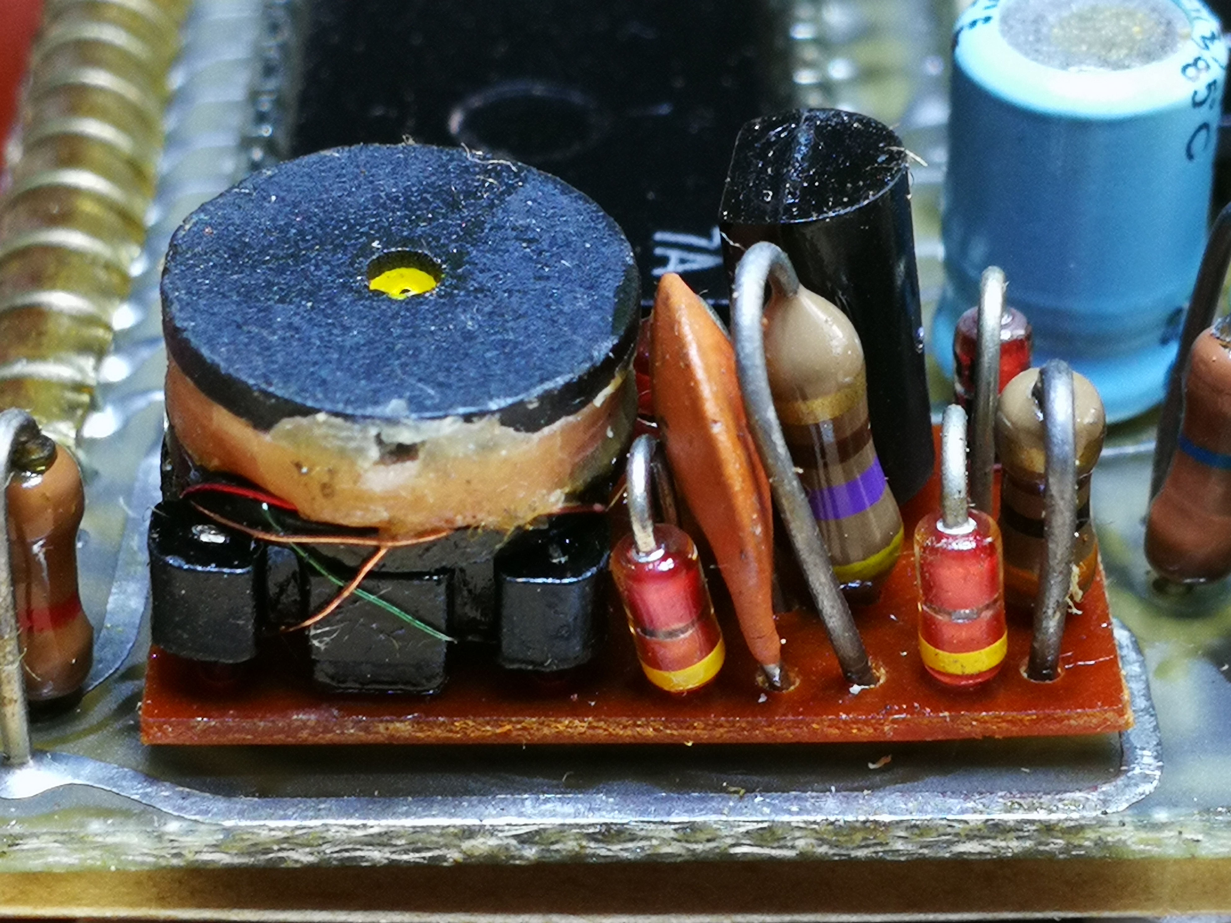
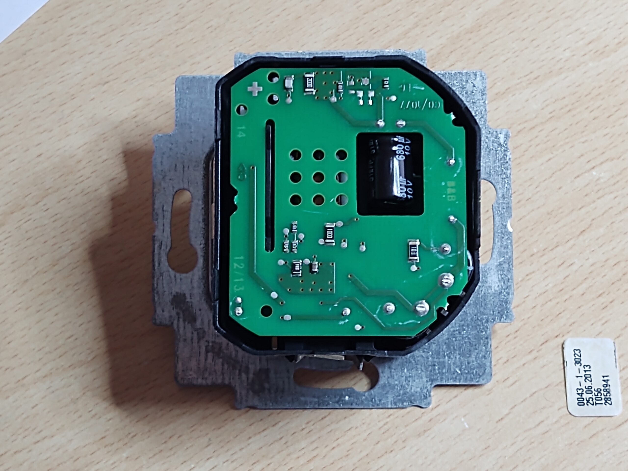
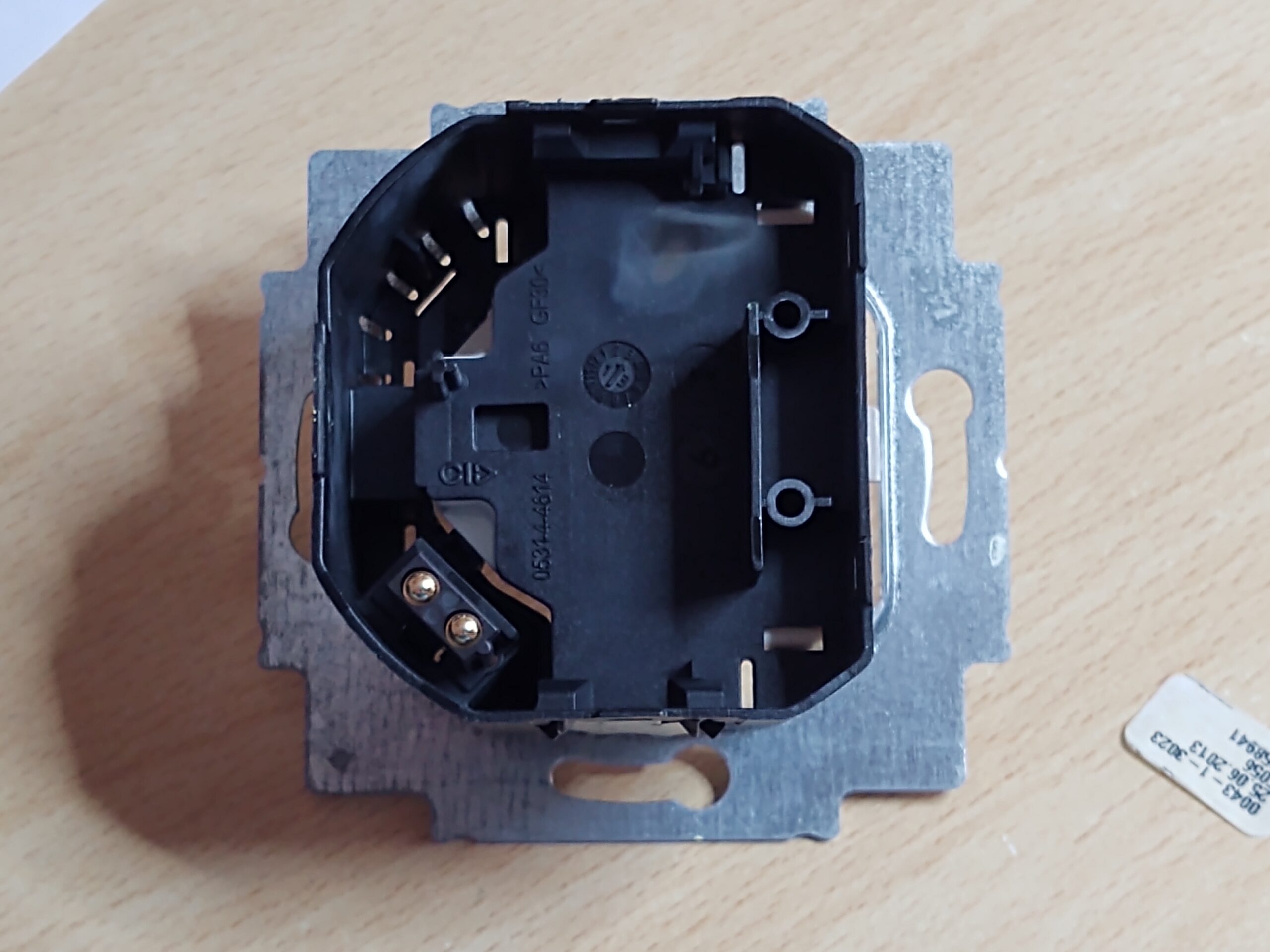
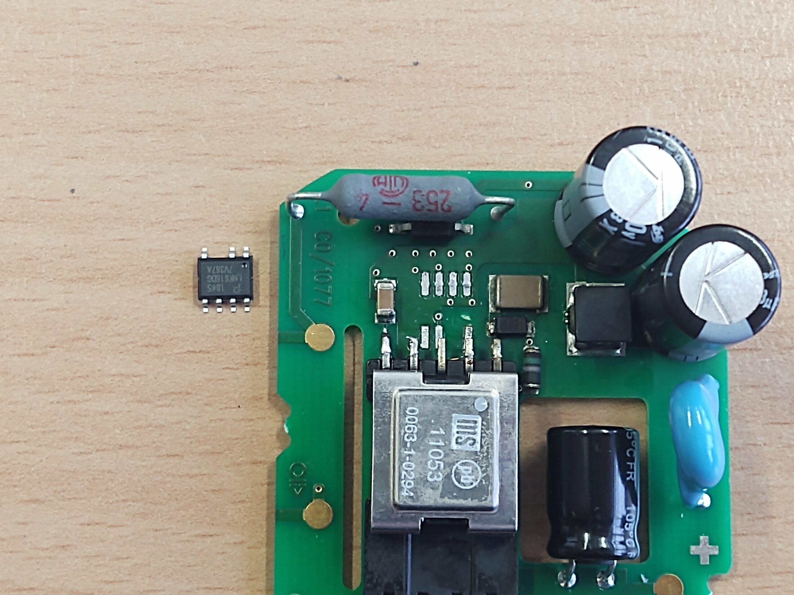
After removing the socket, it was also quickly dismantled. The plastic cover attached to the rear is held in place on the opposite side by means of locking lugs. Now a circuit board came out that can be easily pulled out. The contact to the network side and also to the USB socket is realized via spring contact pins. It should be mentioned right away – they fall out quickly. That is why you should always work the socket with the back facing up. This saves you the hassle of searching for the little pens.
cover removedSocket without power supply board
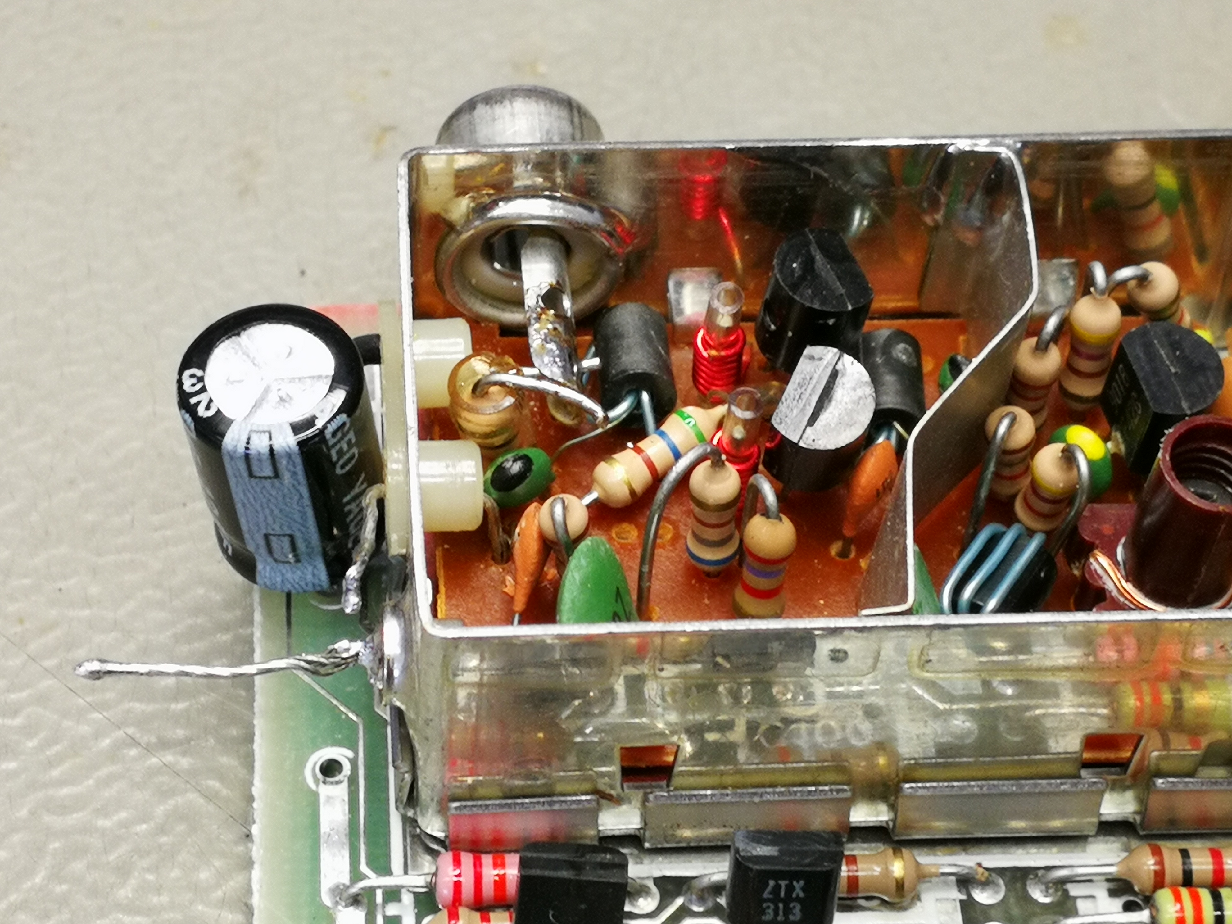
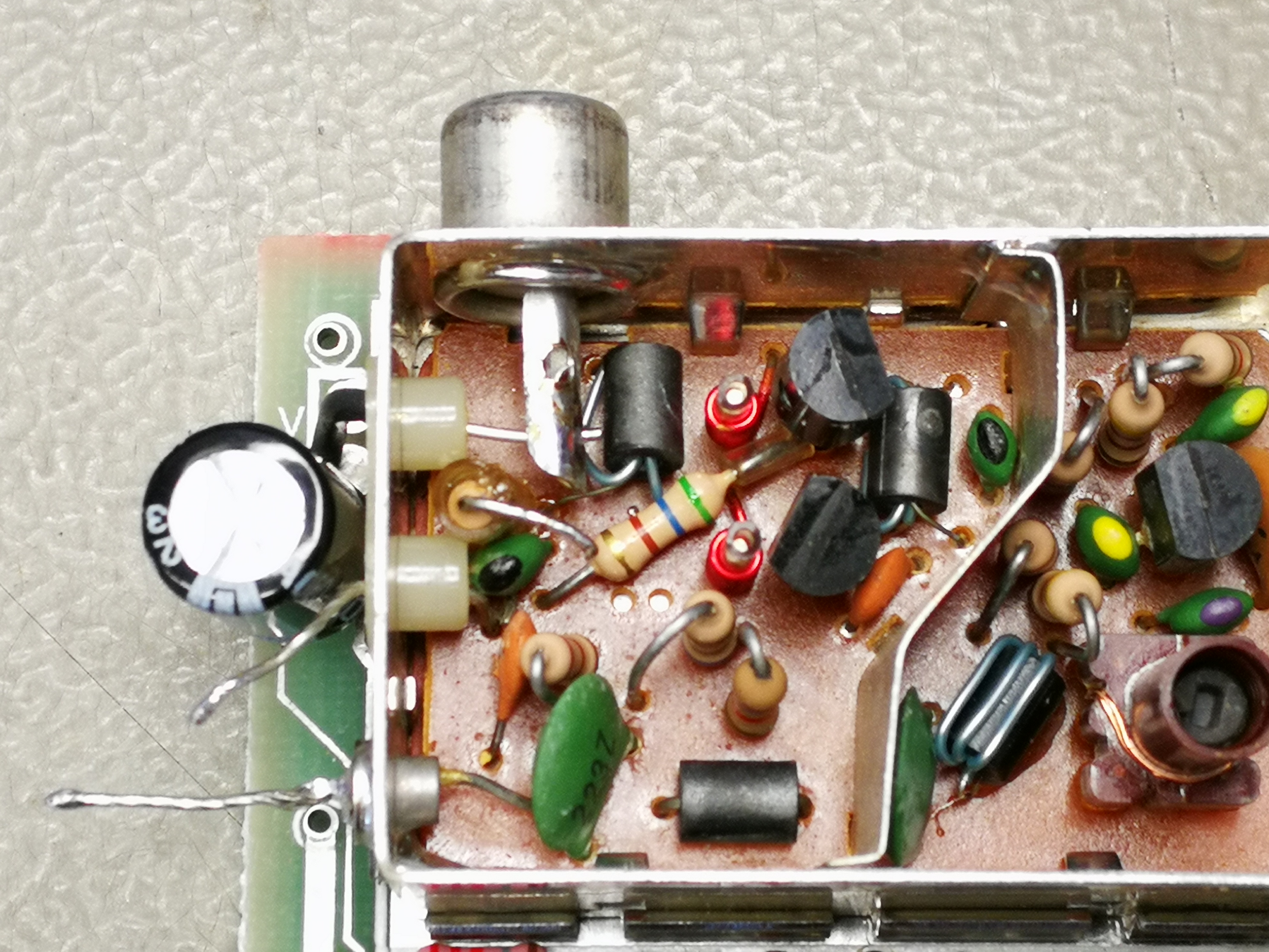
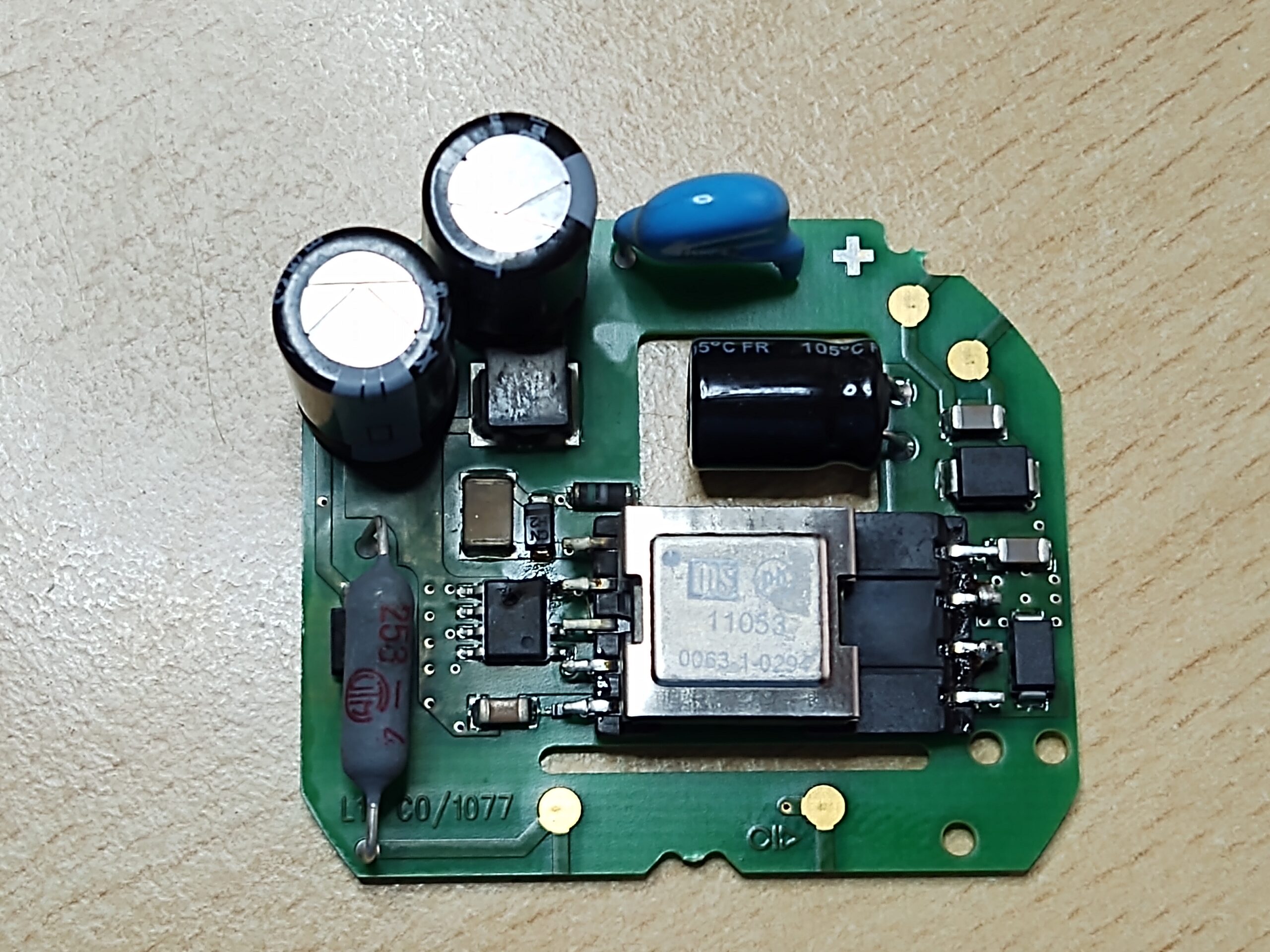
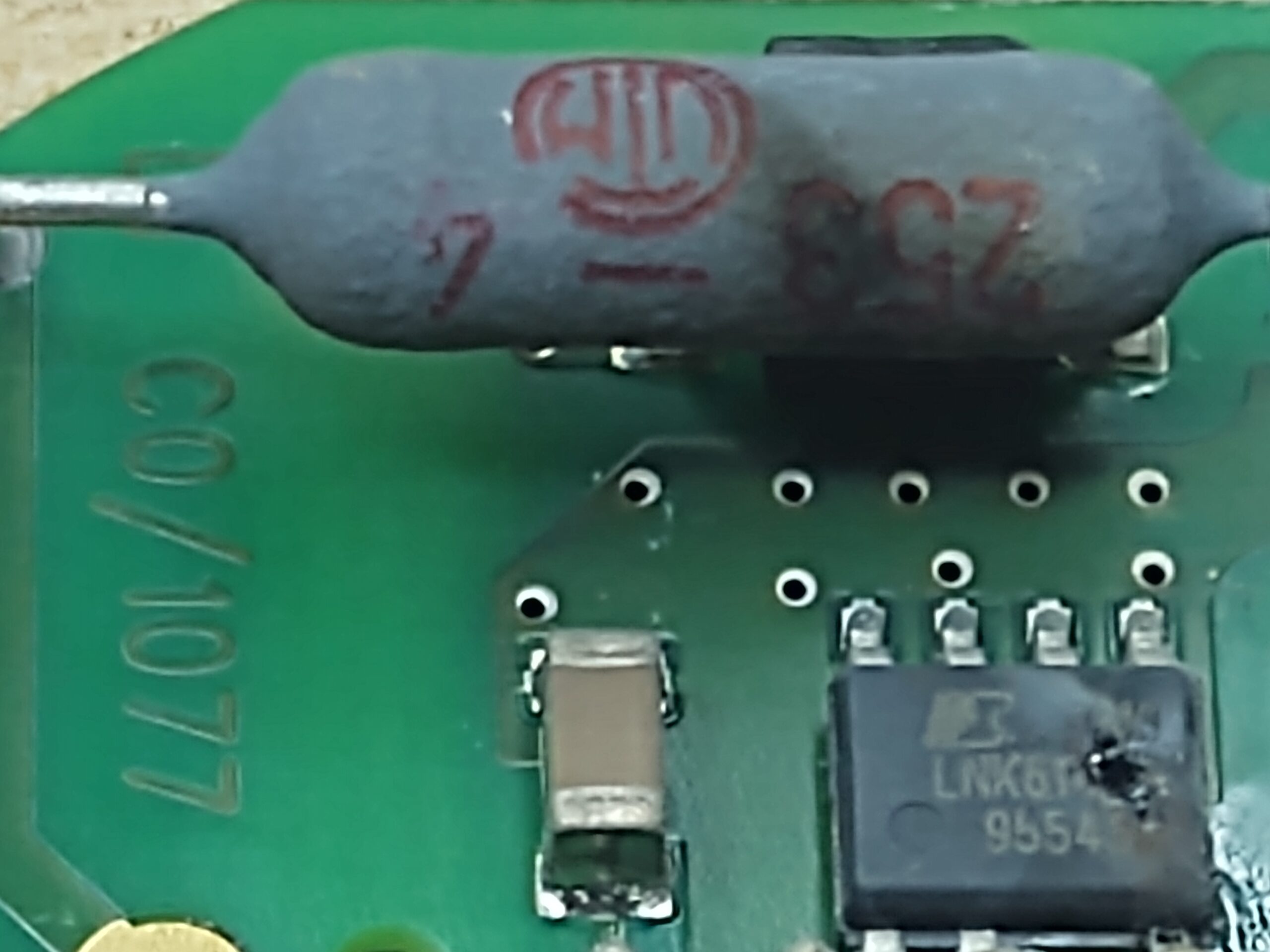
When the board was now released from its housing, at least one problem was revealed, which explains the failure of the power supply. A small chip on the board had a hole that definitely doesn’t belong there. The components surrounding it also showed traces of smoke. Thanks to another functioning socket of this series, I was able to identify the IC.
Power supply boardthe hole in the IC doesn’t belong there“Gunsmoke traces” on the resistance
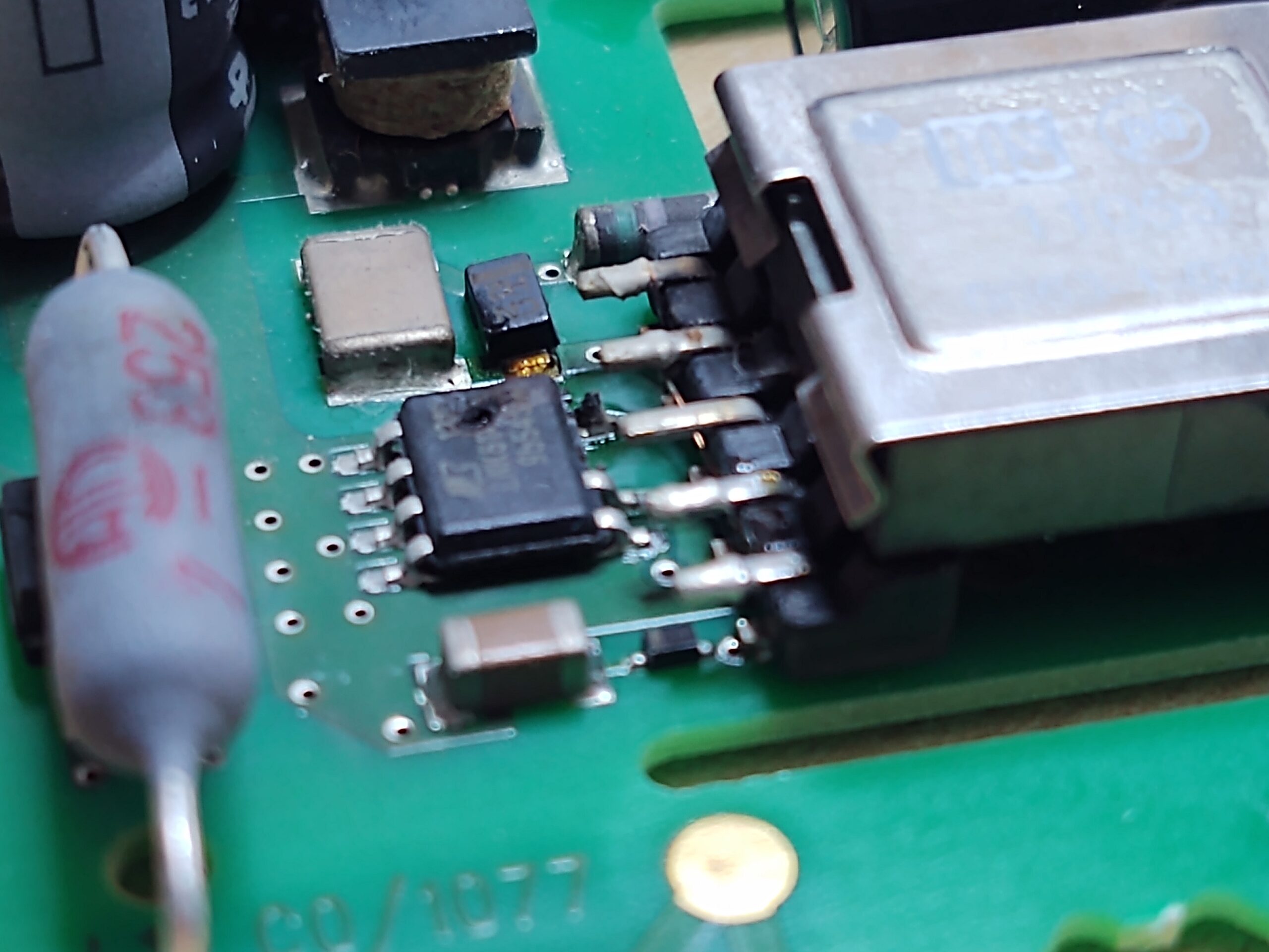
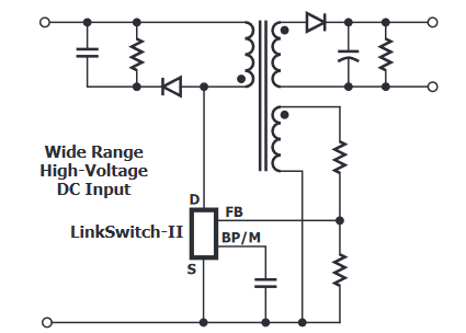
It is a Link Switch-II series LNK614DG from PowerIntegrations. It is a small ALL-IN-ONE IC that has integrated the power FET, the oscillator and the control via a feedback winding of the transformer. The power rating according to the data sheet is 3.5W installed in a closed housing and 4.1W in an open frame or ventilated state.
The chip therefore only needs a few peripheral components, which in this case also makes it easier to search for further errors. On the network side, only the AC rectification and smoothing as well as the line filtering are necessary. These components were in top condition and worked. Then there is only the transformer with its primary, secondary and feedback winding, the secondary rectification and smoothing and a few resistors that are connected as a divider. No fault was found with any of these components. So – who dares wins – the IC ordered and exchanged – and bingo – the 5V are back at the exit and can also be loaded.
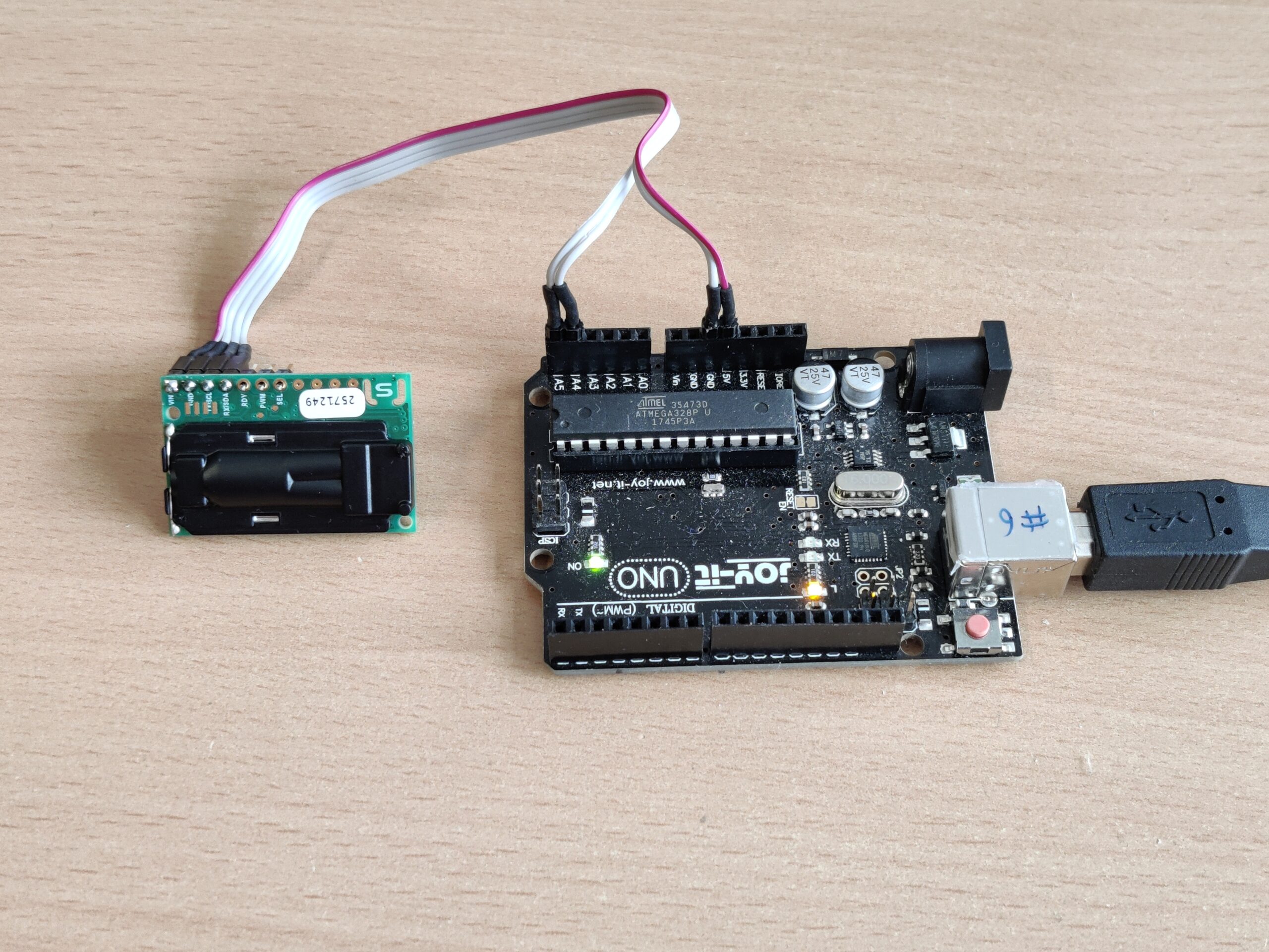
This project – actually a mini project – might also be interesting for one or the other. It is the now well-known and frequently used carbon dioxide sensor SCD30 (CO2 sensor) from the manufacturer Sensirion. There are a number of projects that can be found on the internet. As part of a quick test setup, I tried to read out the data from the sensor using an Arduino Uno board in order to then display it in a plot using the Matlab software. The data transfer takes place via the serial interface or via the serial protocol of the USB-UART.
To connect the SCD30 to the Arduino, you need the power supply and the I²C data bus – so in total just four wires. This means that the minimum configuration is fulfilled and the data can be read out.
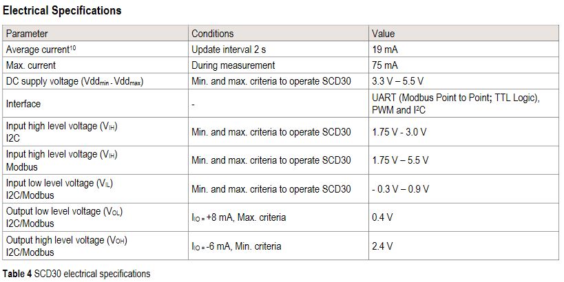
The sensor itself works on the principle of NDIR technology. (NDIR = non-dispersive-infrared). That means the sensor is a small spectrometer. The medium to be examined is fed into a sample chamber. The sample chamber is illuminated by an infrared source and the IR light shines through the medium and a very narrow-band wavelength filter and then hits the IR detector. The wavelength of the filter is designed in such a way that precisely those wavelengths are let through that are absorbed by the molecules of the medium (gas). Depending on the number of molecules or the density of the gas, fewer light beams are recognized by the detector. A second measuring chamber, which is filled with a reference gas, serves as a reference. A controller on the sensor evaluates this information and forwards it in the form of ppm via the I²C (or switchable MOD-Bus) interface. There is also a temperature and humidity sensor on the board, the data of which can also be read out via the bus. The preset I²C address of the SCD30 is 0x61. The exact information on the data protocol can be found in the documentation from Sensirion.
Ideally, as almost always, there is already a ready-made library suitable for students for the various microcontrollers. So you don’t have to worry anymore and can read out the data from the connected sensor directly. The example programs can be found under the examples of the libraries.
electrical specifications
The Arduino with 3.3V or 5V can be used for the supply voltage of the sensor. However, caution is advised when using the I²C bus: Here the input high level is set at 1.75-3.0V and the output high level with a maximum of 2.4V. But on an Arduino the levels are 5V !! So a level shifter has to be built in here – or at least, suitable resistors for a quick test.
The program code listed here essentially comes from the example of the library by Nathan Seidle from SparkFun Electronics:
/*By: Nathan Seidle SparkFun Electronics Library: http://librarymanager/All#SparkFun_SCD30 */#include <Wire.h>#include "SparkFun_SCD30_Arduino_Library.h"
SCD30 airSensor;
voidsetup()
{
Wire.begin();
Serial.begin(9600);
//Serial.println("SCD30 Example");
airSensor.begin(); //This will cause readings to occur every two seconds
}
voidloop()
{
if (airSensor.dataAvailable())
{
// Serial.print("co2(ppm):");
Serial.print(airSensor.getCO2());
//Serial.print(" temp(C):");
Serial.print(",");
Serial.print(airSensor.getTemperature(), 1);
// Serial.print(" humidity(%):");
Serial.print(",");
Serial.print(airSensor.getHumidity(), 1);
Serial.println();
}
else//Serial.println("No data");
delay(500);
}
With these lines of code in the Arduino Uno and the correct wiring (SDA -> to Arduino A4 and SCL -> to Arduino A5 via a suitable level converter) you can continue with Matlab. The Arduino should now output the following lines in a serial terminal: (example)
473,28.5,12.9
473,28.5,13.0
470,28.5,13.1
469,28.5,12.9
466,28.5,12.9
465,28.5,12.7
465,28.5,12.5
463,28.6,12.6
461,28.6,12.5
463,28.5,12.4 … und so weiter
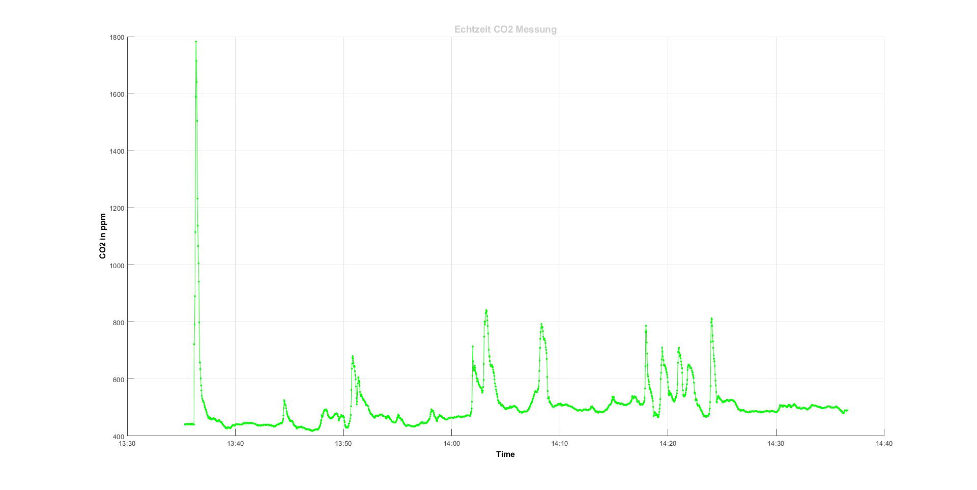
This now has to be read into Matlab and recorded over a definable period and at the same time displayed in a plot. The matlab script here makes it possible … (pn if someone needs it)
The result is a plot that shows the course of CO2 in the room (in this case on my office desk).
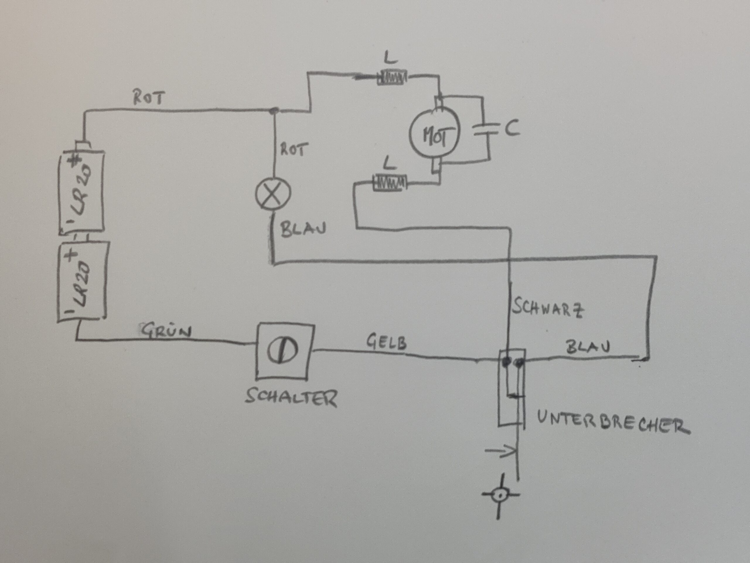
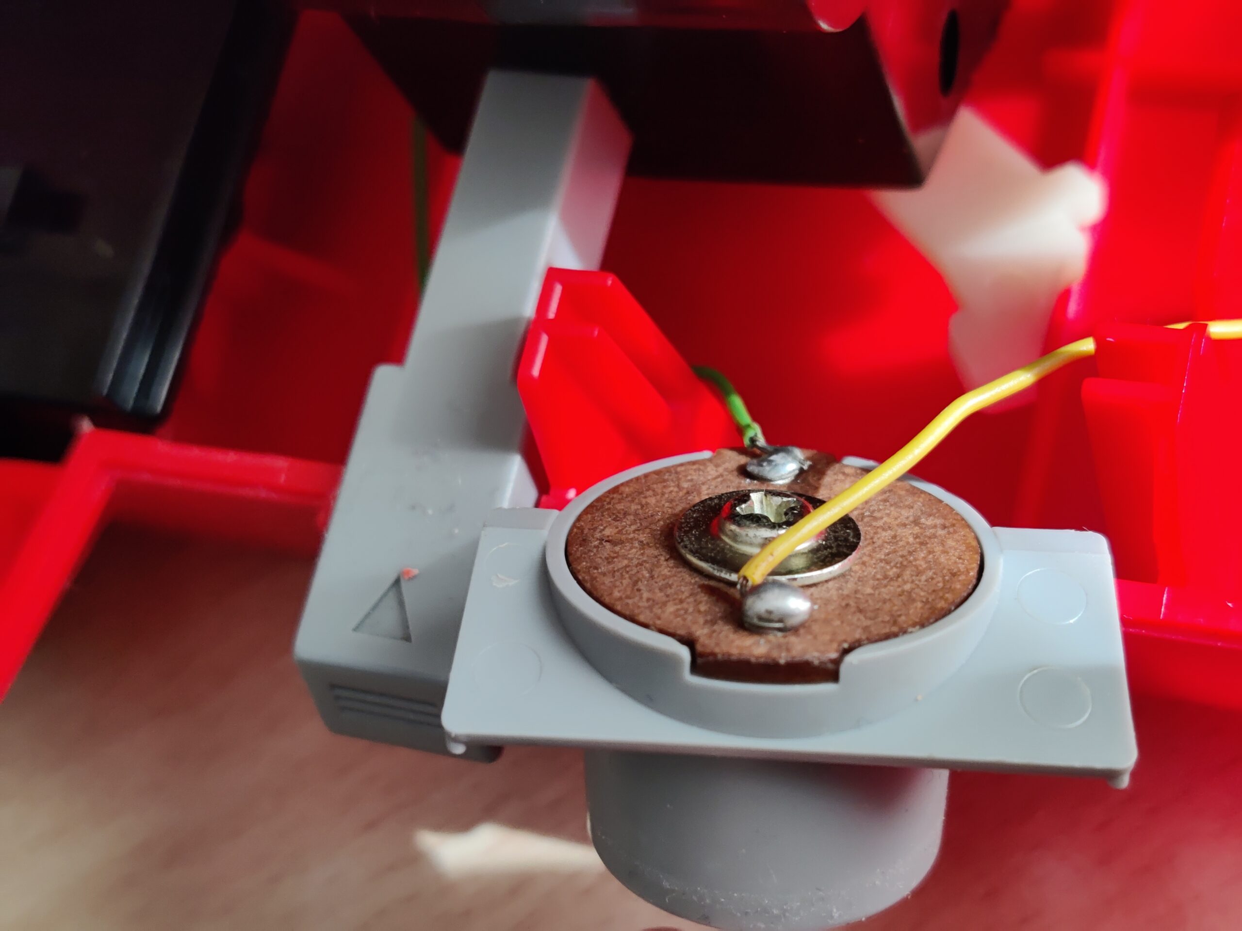
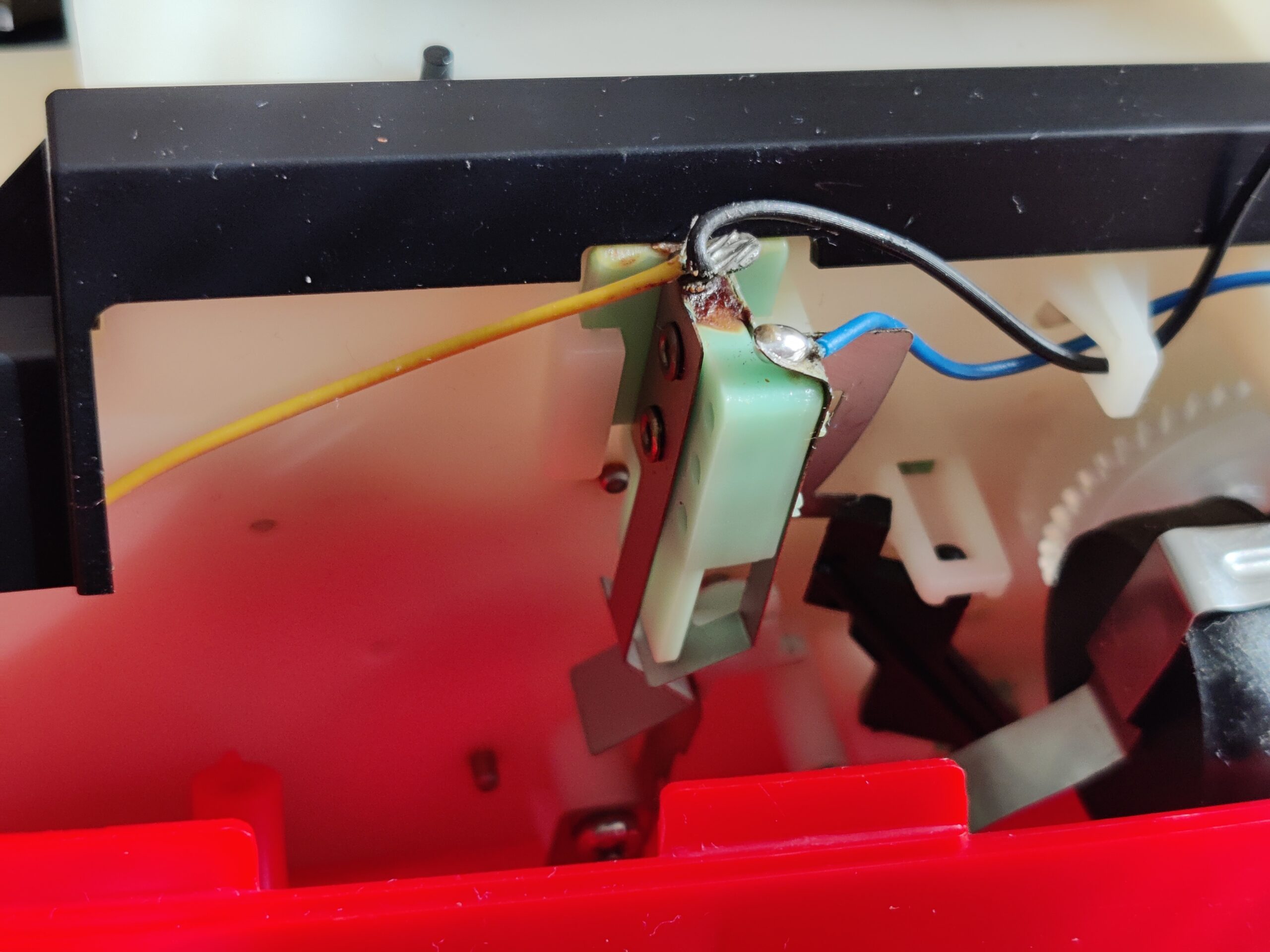
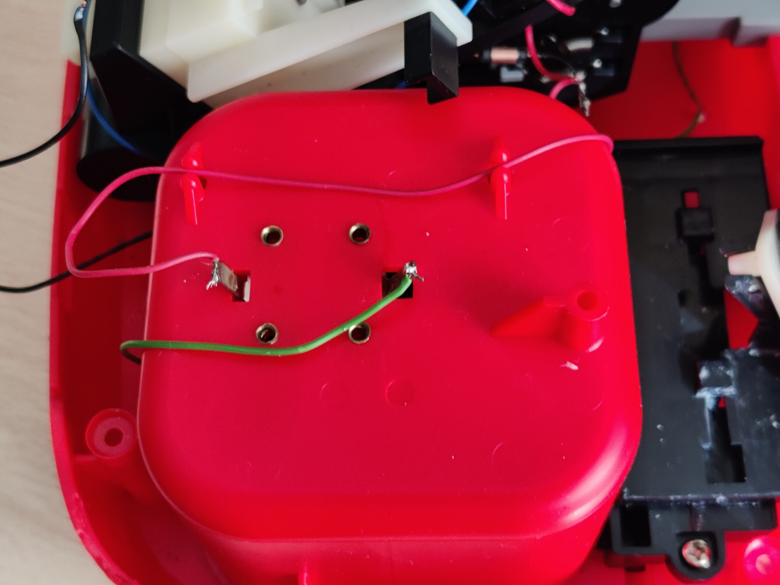
Due to some inquiries regarding the electrical wiring of the Tomy Racing cockpit, I sat down and drew out the wiring. There are apparently many contemporaries who still find toys from the 80s in their basements, attics, etc. and repair them again. With the Tomy Cockpit it happens again and again that the thin wires break off when they are dismantled or the soldered joints no longer hold, often forgotten cells in the battery compartment have dissolved and the contacts and soldered joints are corroded as a result.
I show a sketch of the wiring in the following figure.
By the way, I only use two 1.5V cells, since the parallel connection of two cells each in the battery compartment is nonsense, as the cells are guaranteed to have different internal resistances and thus comfortably discharge each other even when they are not used.
In order to be able to identify the components shown in the sketch in the racing cockpit, I also took photos of them.
This is the back of the “switch” that represents the cockpit’s ignition lock and with which the system is switched on.
I called this part “breaker” because it is a normally closed contact that is triggered by a small “gearwheel” and causes the drum lighting to flash. That happens when you leave the “street”.
These are the connections of the battery box. I doubt whether the colors of the wires are the same for all versions. Because in the devices that I have since revived, different wire colors were installed.
With this information it should now be a little easier to recreate the broken wires and solder joints.
Behind the title mentioned in the article headline is my idea of tidying up the “ingmarsretro” blog and tidying it up a bit. By “cleaning up” I mean checking the individual posts again for spelling errors, maybe reformatting one or the other post and adding to it. That is why there will be no other contribution in January 2021.
There are also plenty of new posts that are digitally saved on the server, but there is no paper version of them yet. So I want to put all the posts that have been created since the last backup back on paper in the form of a book. And unfortunately that is not done in a jiffy, but requires a lot of work. The job and the “family time” with my little son only allow me to work on the contributions mostly at night. And between the posts I also work on the projects (little projects) that I then write about. I also have a lot of them in my head that may one day be realized. And then there are some that I’m working on that are still to be completed, or at least should be continued.
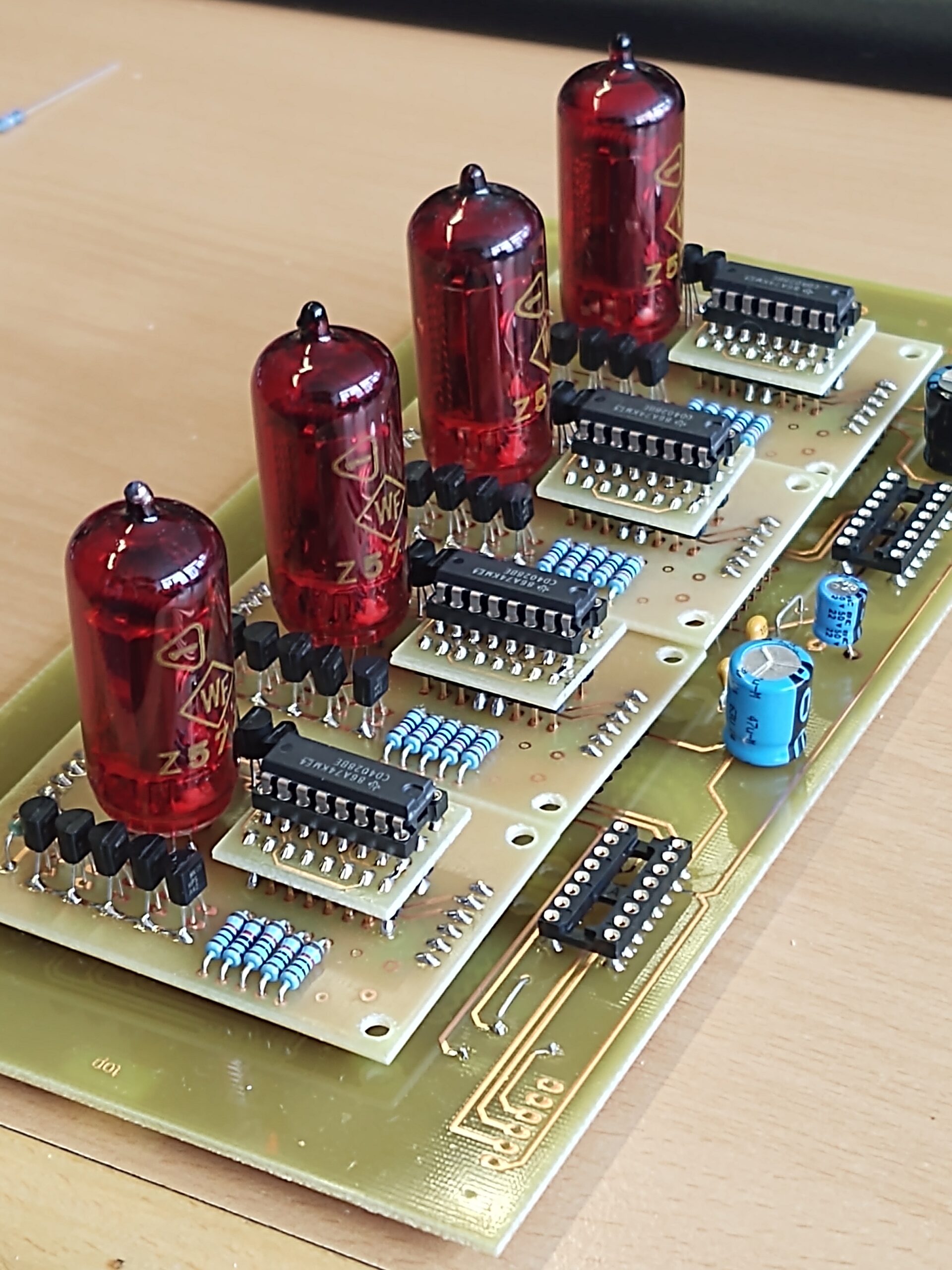
For the last few months I have been working on a Nixie clock that should be set up fairly discreetly. The watch has meanwhile also achieved a reasonable status, so that circuit boards from self-etched prototypes to reasonable, industrially manufactured condition have been created here.
the Nixie clock prototype
The “tube radio receiver” that I started with a few years ago is also waiting to be tinkered with.
Of course, the topic of retro computers does not let me go either. Here are a few devices left to restore and wait to be brought back to life. (This is where I remember right away: I’m looking for a RUN / STOP button for a Commodore Plus 4 – I would be happy if any reader could help …)
looking for a RUN / STOP key
The project with the MOS8501 CPU as a lattice – FPGA – mini board is also in the “carry on queue”. There is still a lot to do here (the level shifters are not doing as they should, the VHDL code still needs to be adapted, the prototypes Circuit boards have to be combined on one board and then also miniaturized …) So there is still enough to do.
Then there are also old devices that I would like to present here in the blog and a number of repairs that keep falling into my hands … Also one or the other HomeMatic tinkering is still pending.
I also toyed with the idea of publishing content from the blog in the form of videos on YouTube. On the one hand, however, I cannot assess whether someone is interested and whether I would like to do that to myself, to present my face in front of the camera. It would probably make more sense to do it with a more didactically gifted person as the protagonist. And of course for Lau, as fun. On the other hand, there are quite a few Youtubers here who are very experienced here (e.g. Dave Jones with his EEVblog, NoelsRetroLab, Adrian’s Digital Basement, GreatScott, ZeroBrain, JanBeta, etc.) and have been doing this for a long time. Also not to be neglected is the immense effort involved in producing such films. When I look at my assembly videos here: It takes almost one day to record the raw material when soldering the respective kit and, in total, almost three days for the cut and post-processing. Let’s see if something can come of it one day …
After the great success of my first book on the retro blog, I have now made my way through and written a second book – NO FUN – there was no success at all. I wrote the book back then in order to have a printed work of my (in) deeds on this website for myself. Because, firstly, it is much more practical to be able to quickly check something – without always having an Internet available and secondly: what if the server (s) can no longer be reached, or is deleted, or even burns down? Or worse, if someone wipes the internet… 😀
At the time I thought to put it on with a “print on demand” option, but who knows if anyone will be interested and if I can even do it that easily. And who would spend so much money on it. Because the individual prints are also quite expensive. So the printed copies presented here are virtually unique. And I’m a little proud of it, because there’s a lot of work to be done.
So now there is the retro book no. 2 with the continuation of the blog entries from the end of the first version to the entry “Schuko socket with USB (repair)” from December 19, 2020 and that is again 96 “stories” which this time cover 498 pages. I chose “epubli” again for this print and ordered it there. This has the advantage that if I want to have one of the existing books printed, I just have to click on “order” again, since all the production data is already there.
I also learned a lot about the formatting of texts, fonts, step sizes and directories. The images are now printed at a higher resolution and all in all it looks better.
So I’ll stay tuned and in a few years, when enough content has been written again, I’ll be working on an issue again.
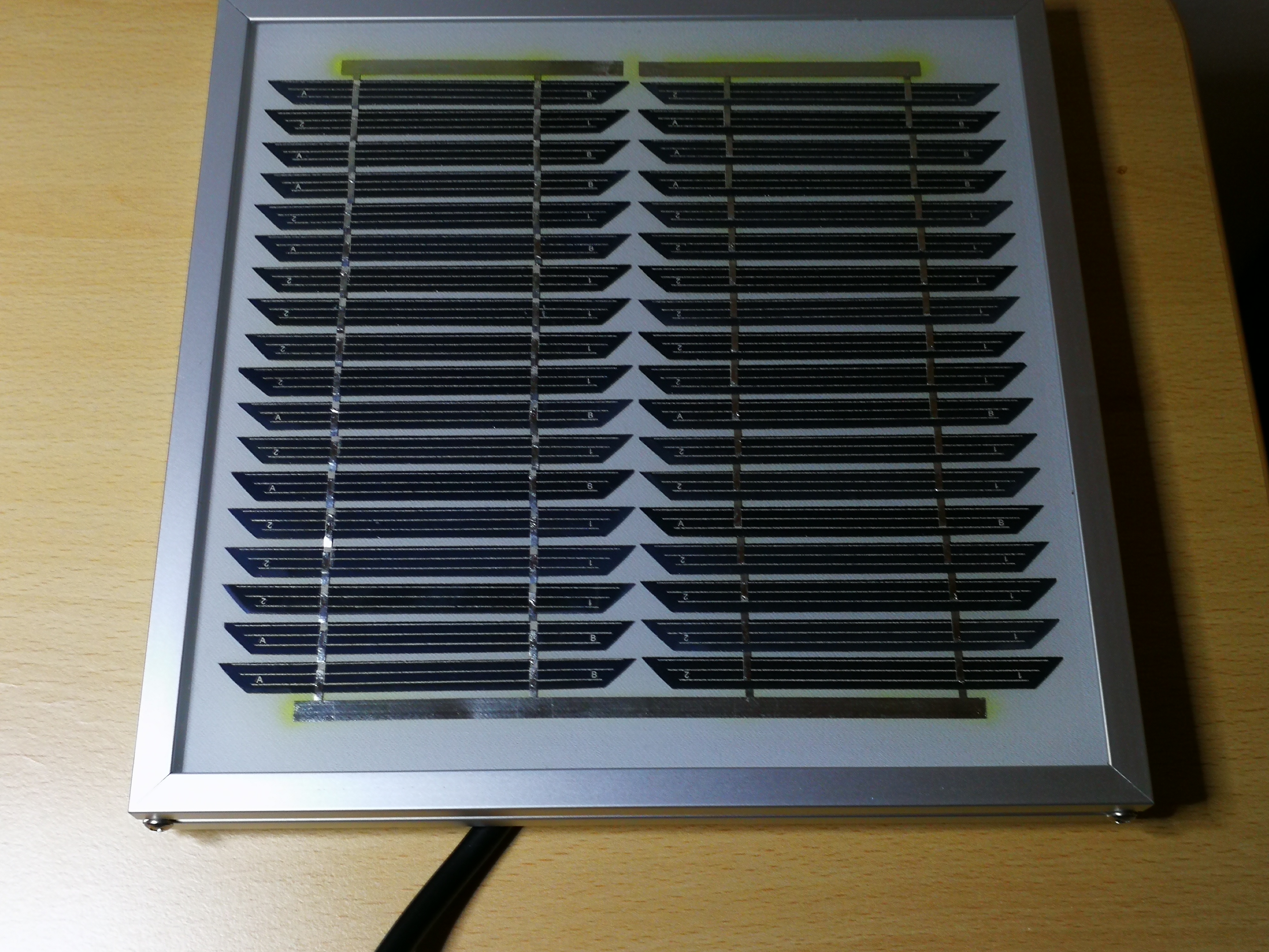
solar module As a mini – craft project for the summertime I call the following tinkering. A small monocrystalline solar module called “SM 6” from a well-known large electronics distributor starting with “C” and ending with “d” plays the main role in the project. The module has a nominal power of 6Wp with a maximum current of 320mA. The rated voltage is 17.3V. The open circuit voltage is 20.8V. The silicon cells are embedded in an EVA (ethylene vinyl acetate) plastic sheet and are UV and moisture resistant. The whole module is about 25cm x 25cm in size. It is thus ideally suited to provide the power to power USB devices. For example, I thought about WIFI IP cams. It should also be possible to charge smartphones or tablets.
In order to be able to do this, the operating voltage of the USB standard (5V) must be generated from the rated voltage of the photovoltaic cell. You could do that easily with a 7805 controller and convert the difference into heat. But this is the least efficient way to get the panel’s energy into a cell phone. Firstly, the internal resistance of the panel depends on the light intensity, which has a major impact on the efficiency of unmatched load resistors. On the other hand, a series regulator is a power shredder, since the difference between input voltage and regulated output voltage is converted into power loss, ie heat, during the flow of current. Here you are better served with a switching converter (buck converter).
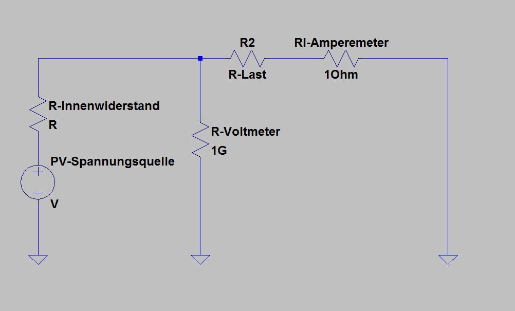
In a simple laboratory setup, the behavior of the panel can be examined. For this purpose, the open circuit voltage of the panel is measured at different illuminance levels. Subsequently, the panel is loaded with different resistance values and the current through the load as well as the voltage at the panel are measured. The measured values are recorded and the Ri (internal resistance of the source) is calculated. The following circuit diagram shows the measurement setup:
measurement setup – schematic
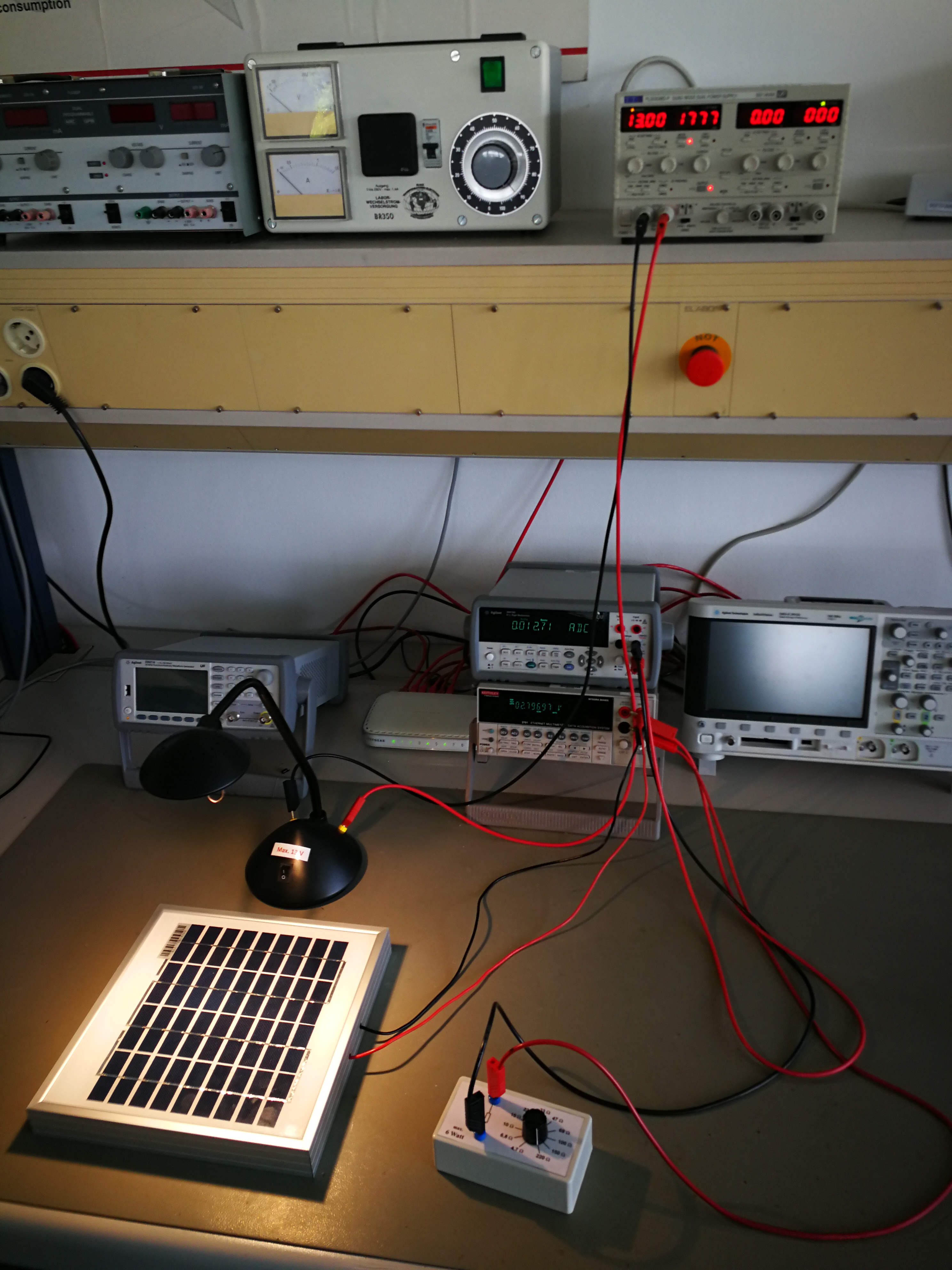
The ammeter is an Agilent and Voltmeter Keithley 2701 table multimeter. These gauges can both be controlled via SCPI commands. The interface is a LAN port. This makes it easy to implement an automated measurement process via a PC and a suitable script. And since Matlab offers a very convenient way to script, it’s also used right now. In order to be able to measure in a laboratory and have approximately the same environmental conditions, a table lamp with halogen bulb is used instead of the sun. The brightness of the lamp is easily adjusted by supplying it with a laboratory power supply of 0-13V. Of course, the laboratory power supply can also be controlled by Matlab.
measurement setup with lamp as “sun”
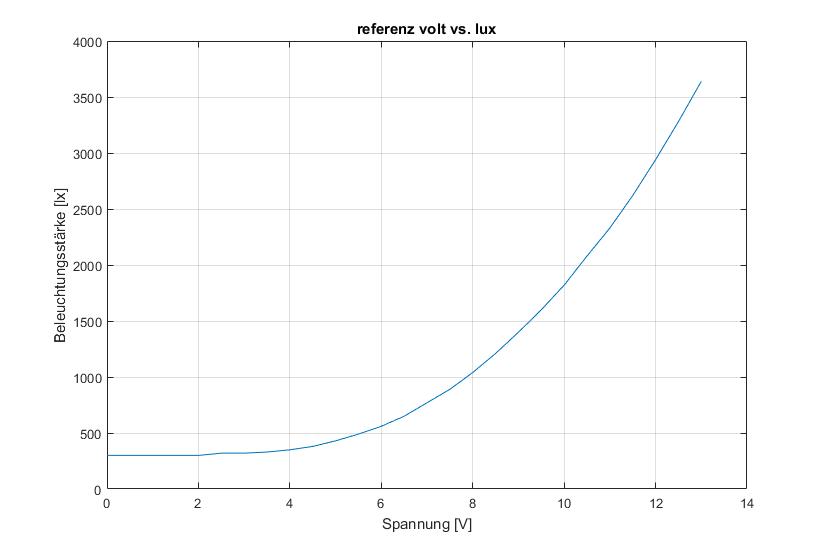
The lamp is placed at a distance of 25cm in the middle of the panel. In order to get a feeling of which illuminance is achieved with the lamp, a reference measurement is taken with a luxmeter. That is, the lamp goes through the power ramp of 0-13V and the lux meter measures the illuminance at a distance of 25cm under the lamp. The whole thing is resolved in 0.5V steps. This results in a curve that looks like this:
Voltage on the lamp results in illuminance
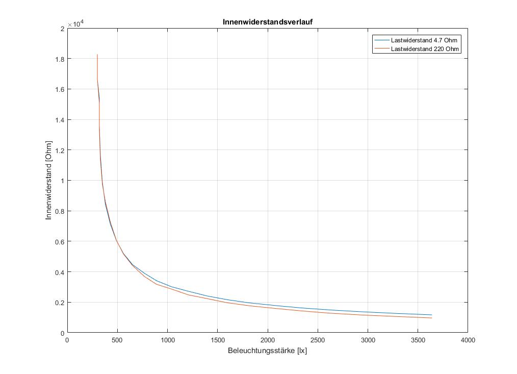
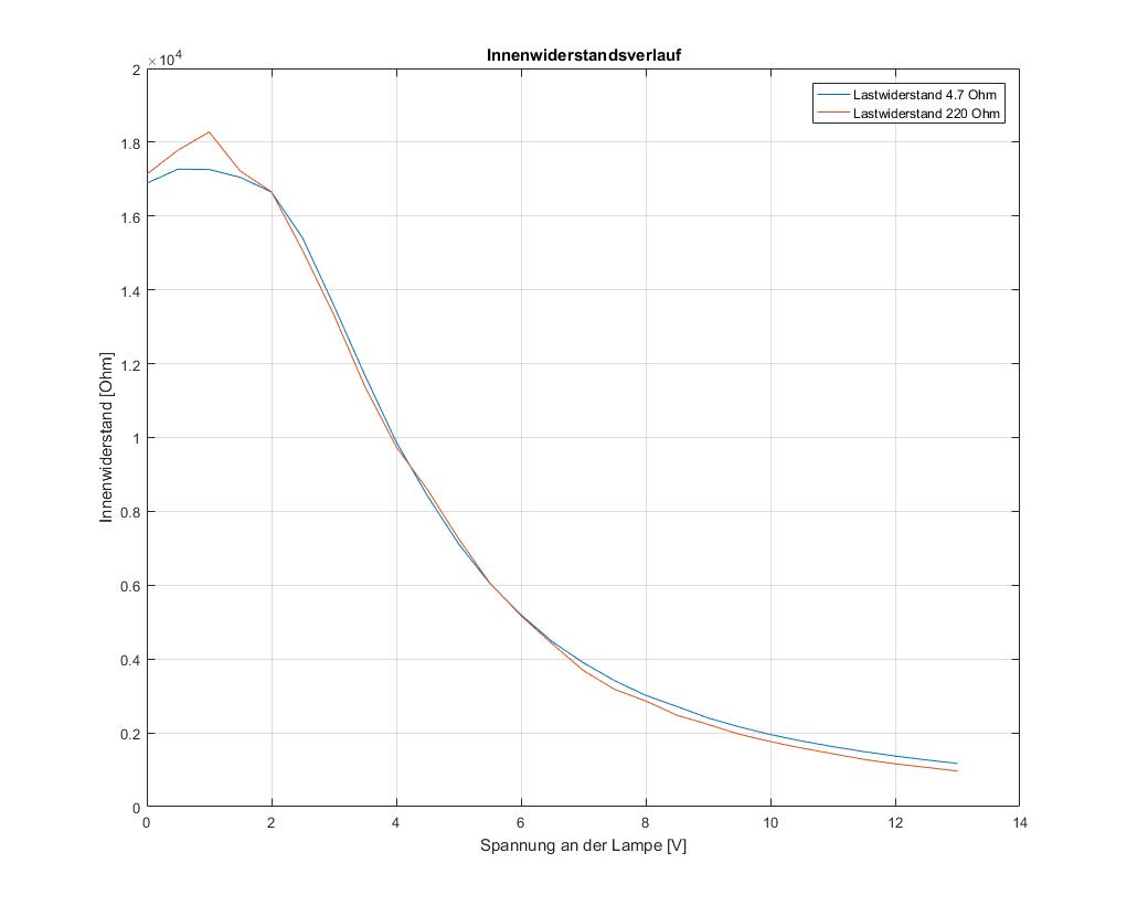
Now the measurement can begin. Resistors are manually connected to the panel as a load resistor and current and voltage are measured at each brightness level. There are eleven load resistance values ranging from 4.7 ohms to 220 ohms connected in sequence. An idle measurement is then of course made without load resistance. The following graph shows the calculated internal resistance for two loads of the panel over the brightness curve of the lamp in lux and in the other graph over the voltage at the lamp (for better scaling). The internal resistance of a source is calculated from the open circuit voltage of the source minus the voltage under load, divided by the current. With the difference between the no-load and load voltage, the voltage drop at the internal resistance is obtained. Since the load is also known as the current, it is only necessary to use Ohm’s law to obtain the resistance value …
Internal resistance vs. illuminance Internal resistance vs. Voltage on the lamp
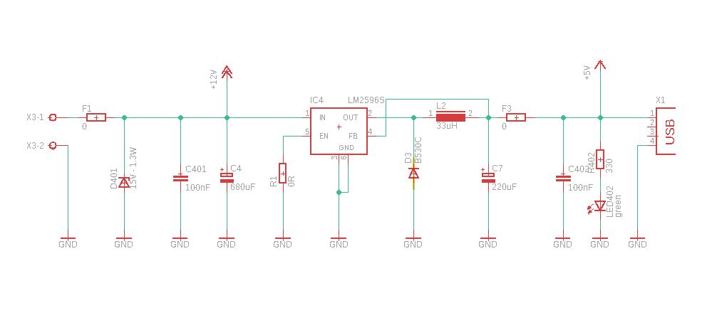
Since some clarifications about the behavior of the PV cell have now been eliminated, I can briefly report on the structure of the voltage converter. As previously announced, a switching converter is the more efficient way to adapt the energy to the consumer. Here comes an LM2596S used. The LM 2596 is a “Simple Switcher Power Converter” that switches at 150kHz and can supply a load with 3A.) Here is an overview of the functions:
3.3-V, 5-V, 12-V, and Adjustable Output Versions
Adjustable Version Output Voltage Range: 1.2-V to 37-V ± 4% Maximum
Over Line and Load Conditions
Available in TO-220 and TO-263 Packages
3-A Output Load Current
Input Voltage Range Up to 40 V
Excellent Line and Load Regulation Specifications
150-kHz Fixed-Frequency Internal Oscillator
TTL Shutdown Capability
Low Power Standby Mode, IQ, Typically 80μA
Uses Readily Available Standard Inductors
Thermal Shutdown and Current-Limit Protection
(source: datasheet from vendor TEXAS Instrument)
With this switching converter and a few other components can quickly assemble a circuit and transform with the layout tool “Eagle” into a board. However, this circuit is so simple that it only works as efficiently as possible with the advantages of the LM2596, but does not perform any power tracking. This means that the load representing the circuit for the solar cell is not adapted to the internal resistance of the solar cell.
Circuit diagram of the DC-DC converter
From this circuit, a simple layout was created, a board etched and equipped. A USB socket on the output allows the direct connection of USB devices. To make the whole thing look a bit reasonable, I have donated the board still a small plastic casing …
Measurement of illuminance
measurement setupSwitchable load resistorsLayout on the computerFoil for creating the printed circuit boardEtched PCBEtched PCBFinished circuitCircuit diagram of the DC-DC converter
A simple layout was then created from this circuit, a circuit board was etched and assembled. A USB socket at the output enables direct connection of USB devices. To make the whole thing look a little sensible, I donated a small plastic housing to the circuit board …
Messung der Beleuchtungsstärke
Measurement setupSwitchable load resistorsLayout on the computerFoil for creating the printed circuit boardEtched PCBAssembled PCBFinished circuit
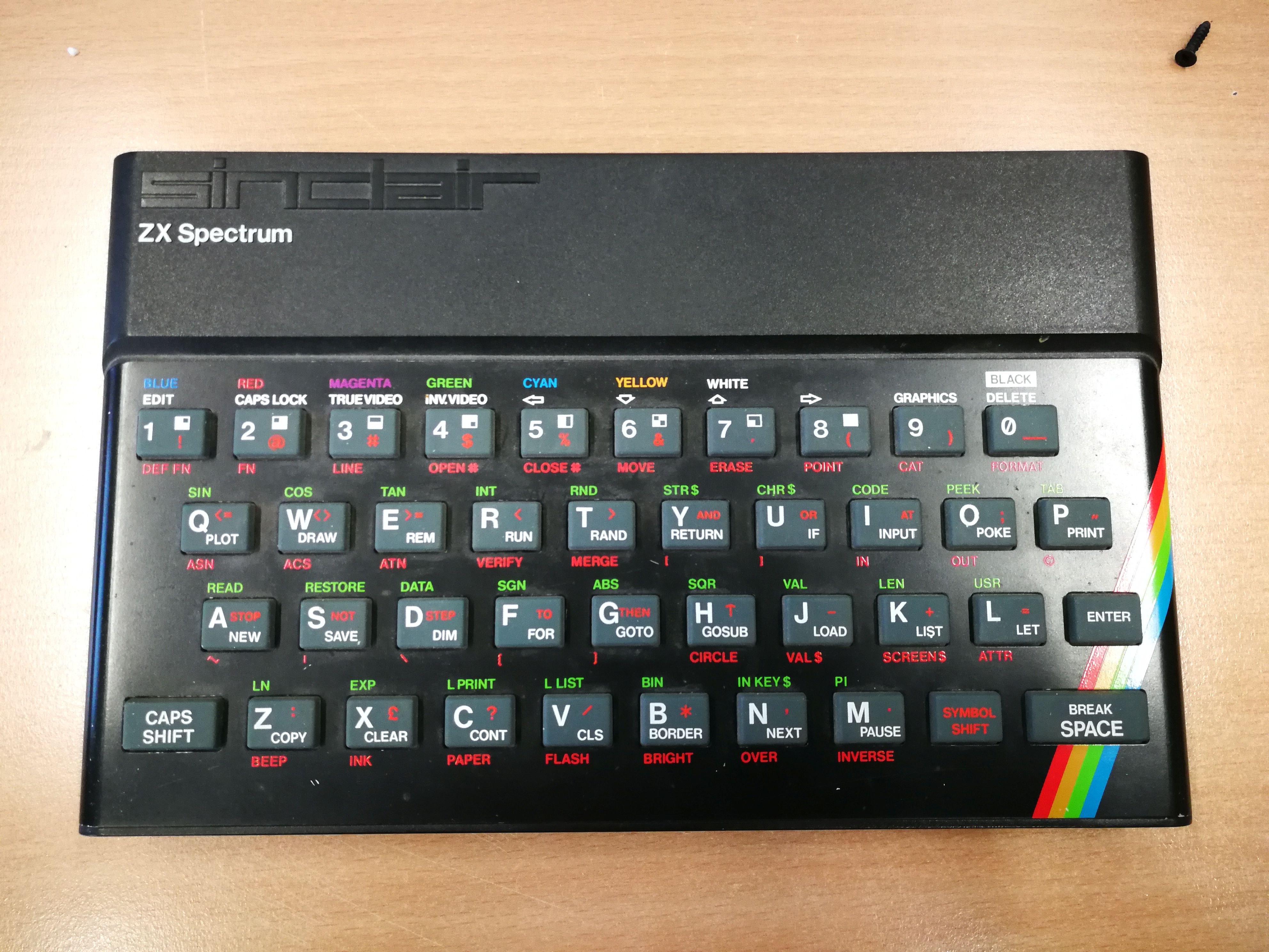
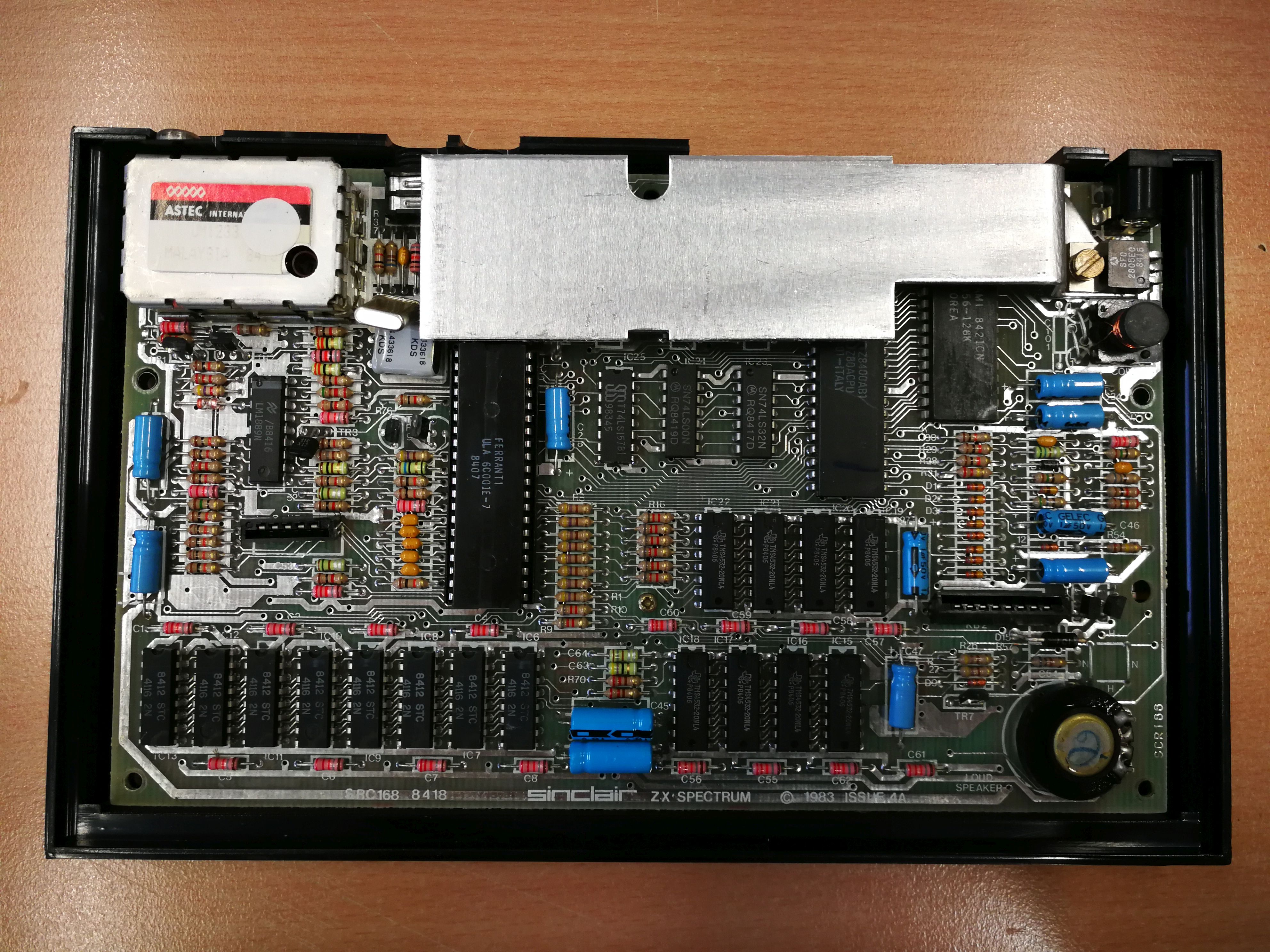
On April 23, 1982, the Sinclair ZX Spectrum has been marketed by Sinclair Research. [Source: Wikipedia] He was then sold at a price of 140 euros or 194 euros. The two prices refer to the 16kByte version or the 48kByte version. 16kByte and 48kByte are the sizes of the RAM memory with which the computers were equipped. The ZX-Spectrum is the successor to the Sinclair ZX81 and the predecessor of the ZX-Spectrum Plus and Sinclair QL.
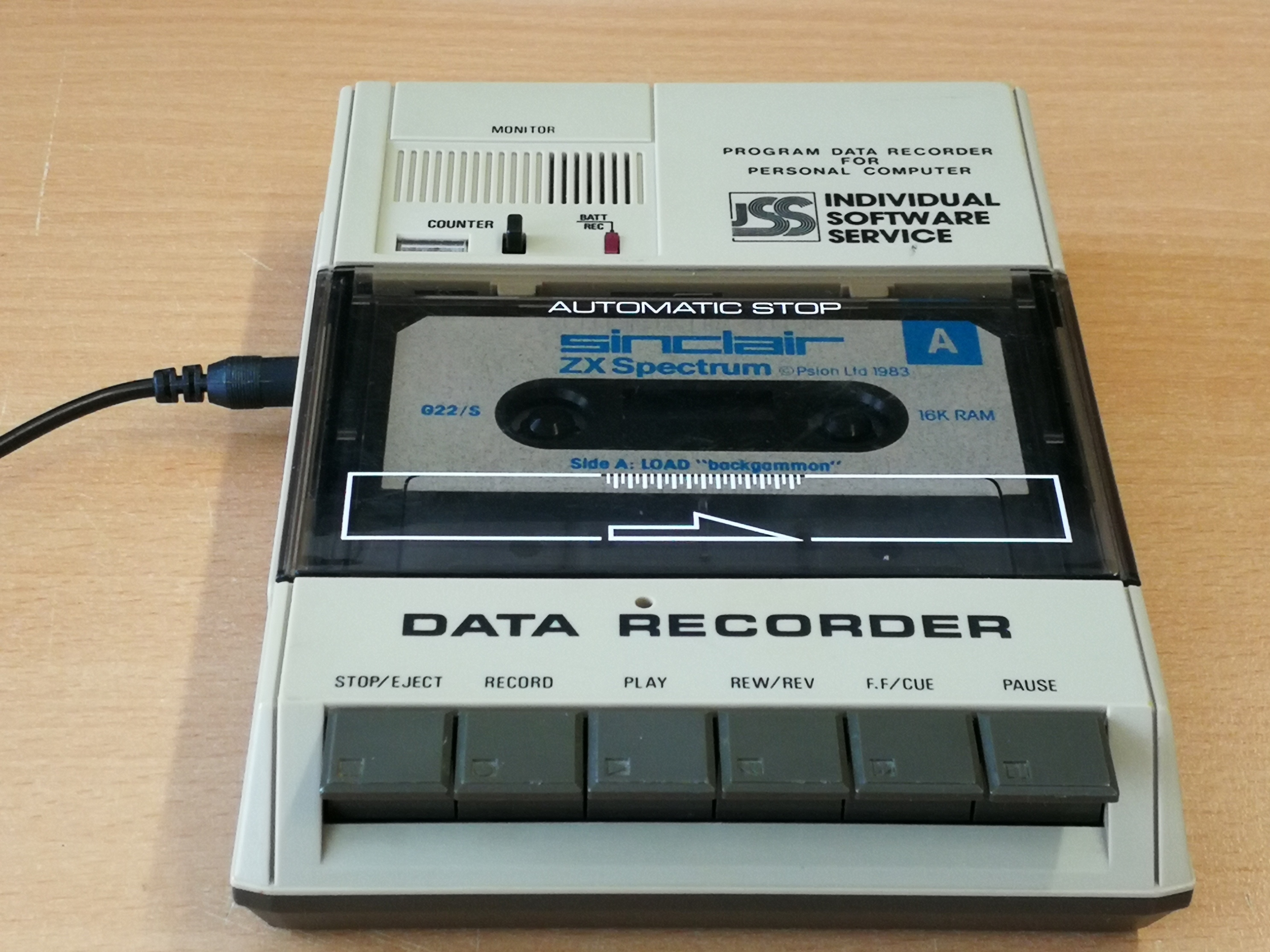
The small computer (the dimensions are just 23.5cm * 14.5cm * 3cm) is powered by a Z80A CPU running at 3.5MHz clock speed. The ULA (Uncommitted Logic Array) is the largest chip on the ZX motherboard. She is responsible for the graphics, the audio IOs (for loading and saving programs on tape) and keyboard input. Then there are, depending on the version, the DRAM chips (upper and lower RAM) on the board and another ROM IC, which houses the BASIC interpreter. The small calculator can draw colorful graphics on the screen with a resolution of 256 x 192 pixels and 15 colors. The image output is sent to the antenna input of a TV via a built-in RF modulator. With picture output but I really only the “picture”, because for the sound is not the audio channel of the TV set used. But there is a small speaker on the motherboard, which outputs the sounds of the computer. Which in turn are not generated like in the C64 in a separate chip (SID chip) and that in several voices – no, the MIC / TAPE pin of the ULA is used, which simply switches the speaker via a transistor to 5V. This can then be used to generate simple “beep noises”. Of course, from a current point of view, that’s nothing special at all, but for those who were confronted with it in their childhood, there are certainly some memories associated with it. So also for me. At least then I had the opportunity, with my brother to borrow such a device from a friend. Then of course it was – how can it be otherwise – played. Titles such as “Manic-Miner”, “Ant-Attack” or Flight Simulator were among the most frequently loaded cartridges. Yes – cassettes. At the time it was common to buy the programs on an audio cassette. A simple tape recorder was connected to the ZX-Spectrum via the headphone jack and the LOAD “” keys were entered via the rubber keys on the ZX. Then you had to press on the tape recorder only more play and it could start. The prerequisite was, of course, that the tape speed and the adjusted volume level fit. Only then was the loading of the program successful and the game started. The loading times were from two to often more than ten minutes depending on the program.
datarecorder for loading and saving from programmcode
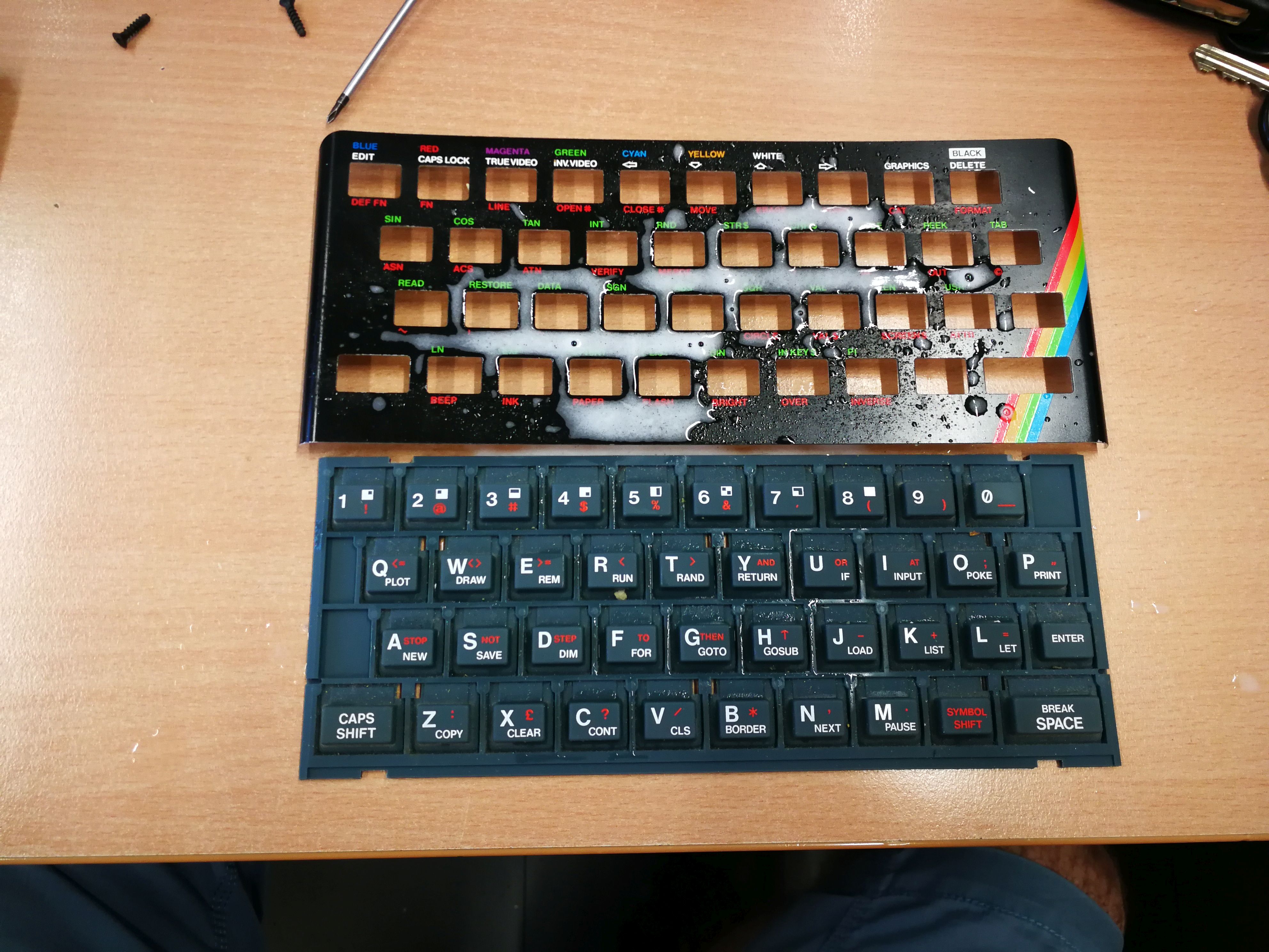
In my 8Bit – Retrorechner collection was missing until now the complete series of Sinclair calculator, but finally I could make a bargain and buy a whole set with ZX-Spectrum, joystick module, a data recorder and many original game cassettes. I would like to briefly describe the preparation and restoration of the ZX here. If you get your hands on a computer with an unknown background, which has been lying around in a cellar for the last 30 years, you should not try to put it into operation. If he is not already, that could be his death. Because, as always, there are some parts that can age and change their parameters. Someone could have tinkered with it before to repair or retool something. In this case, the case was dusty and dirty, but there were no missing screws, dents or externally apparent retrofits, such as buttons or plugs. So I could solve the case screws.
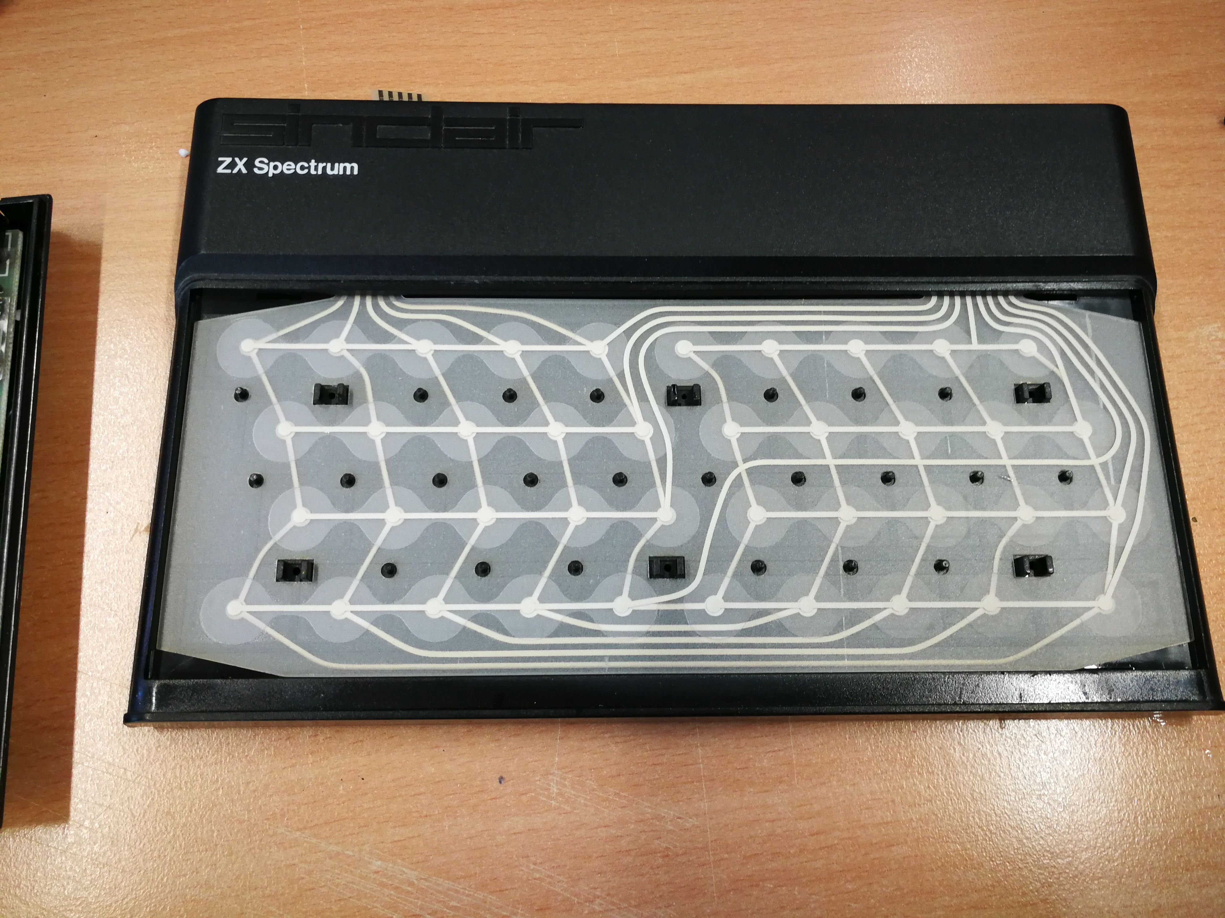
The keyboard foil was quickly pulled out of the clamping bushes and the lid with the rubber keys removed. Now the inner life of the Spectrum revealed itself – and what can I say – 1A. Everything in original condition. No repairs or tinkering have been done on the device yet. So I first started cleaning the body parts. The keyboard is easy to disassemble. In this revision of the spectrum (ISSUE 4A), the metal sheet that holds the rubber mat in the housing is fixed with four “brass bending tabs”. These can be easily bent back and remove the sheet.
Frontblech und Gummitastenmatte enfernt
freigelegte Tastaturfolie
The housing parts were now very easy to clean. I rinsed it with soap under lukewarm water. Also, the residue between the rubber mat buttons could be easily removed. While the parts were now set aside to dry, I dedicated myself to the motherboard.
Mainboard des ZX-Spectrum 48K Issue 4A
Here all solder joints were clean, no traces of foreign intervention and all parts still in original condition. So I could start directly with the first exams. An ohmmeter was used to test for short circuits in the power supply area. If you look at the circuit diagrams of the spectrum, you can quickly see that the computer is supplied with an input voltage of DC9V. Here the assignment of the power supply socket is to be considered. Here, the plus pole is not the inner pin but the outer ring of the connector. This is especially important if the original power supply is no longer available and you take a replacement. The further structure of the supply concept is as follows: From the 9VDC the + 5V supply is made via a linear regulator 7805. Using a DC / DC converter circuit consisting essentially of the components TR4 and TR5 and a small transformer (cylindrical coil with two windings), a 12VDC and further a -5VDC power supply are generated. Special attention should be paid to this area, as a wrong or missing power supply can damage other components (especially the DRAM ICs). To do this, use a diode tester to test the transistors for their conduction and blocking behavior of the PN junctions. The easiest way to test the small transformer is to use the ohmmeter for low-resistance behavior of the respective winding and high-resistance behavior between the primary and secondary windings. If everything is alright here, one tests the output of each of the three voltage sources with respect to the ground 0V potential. Here are the following guidelines to measure:
Eingang des Linearreglers (9V) gegen GND -> ca. 100k-150k
Ausgang des Linearregler (+5V) gegen GND oder an Pin9 des RAM ICs -> ca. 300 – 500 Ohm
Pin1 des RAM ICs (-5V) gegen GND -> ca. 300 Ohm (im 400Ohm Messbereich)
Pin8 des RAM ICs (12V) gegen GND -> ca. 2.6k bis 2.8kOhm
Elektrolytkondensatoren erneuern
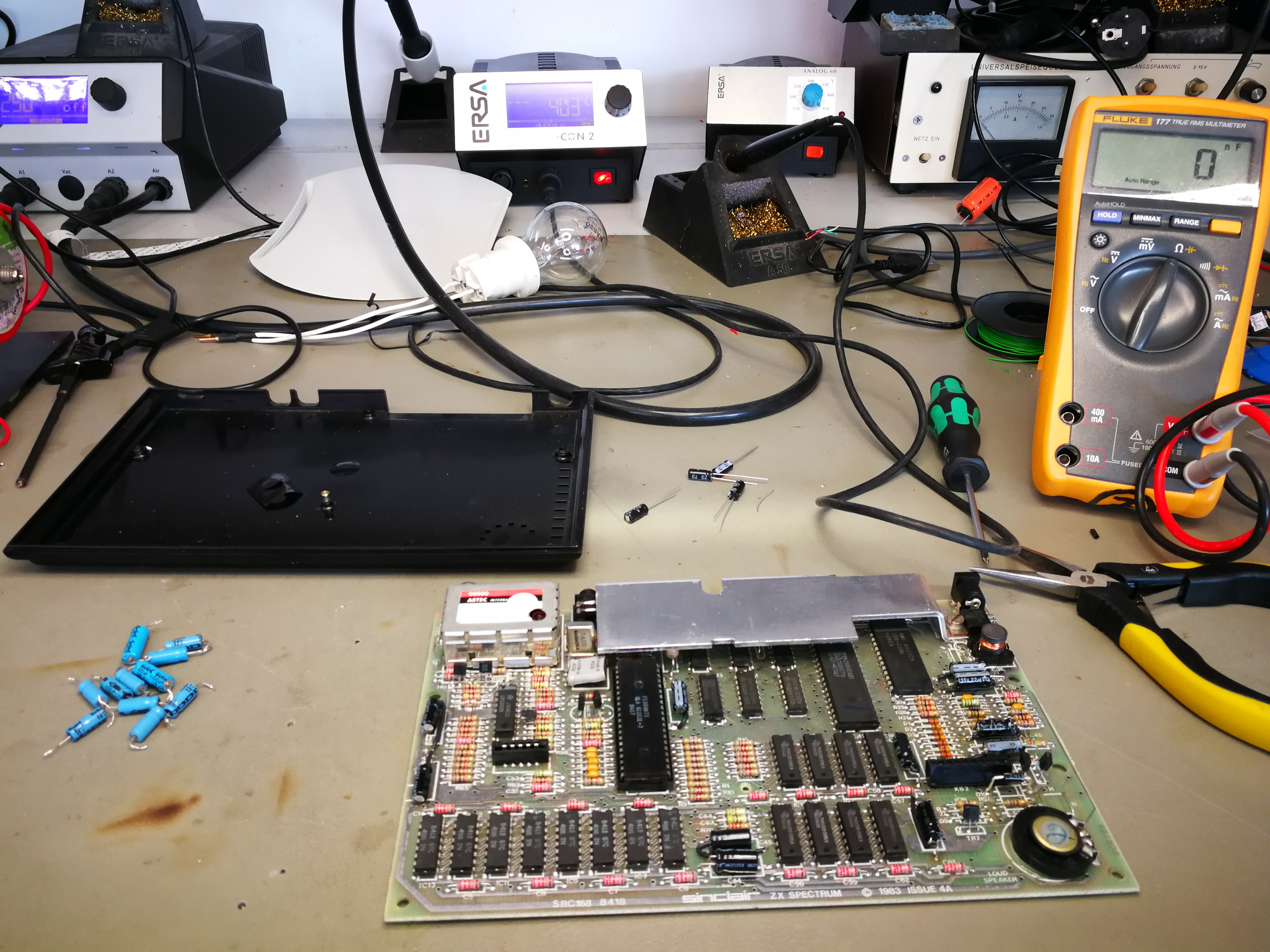
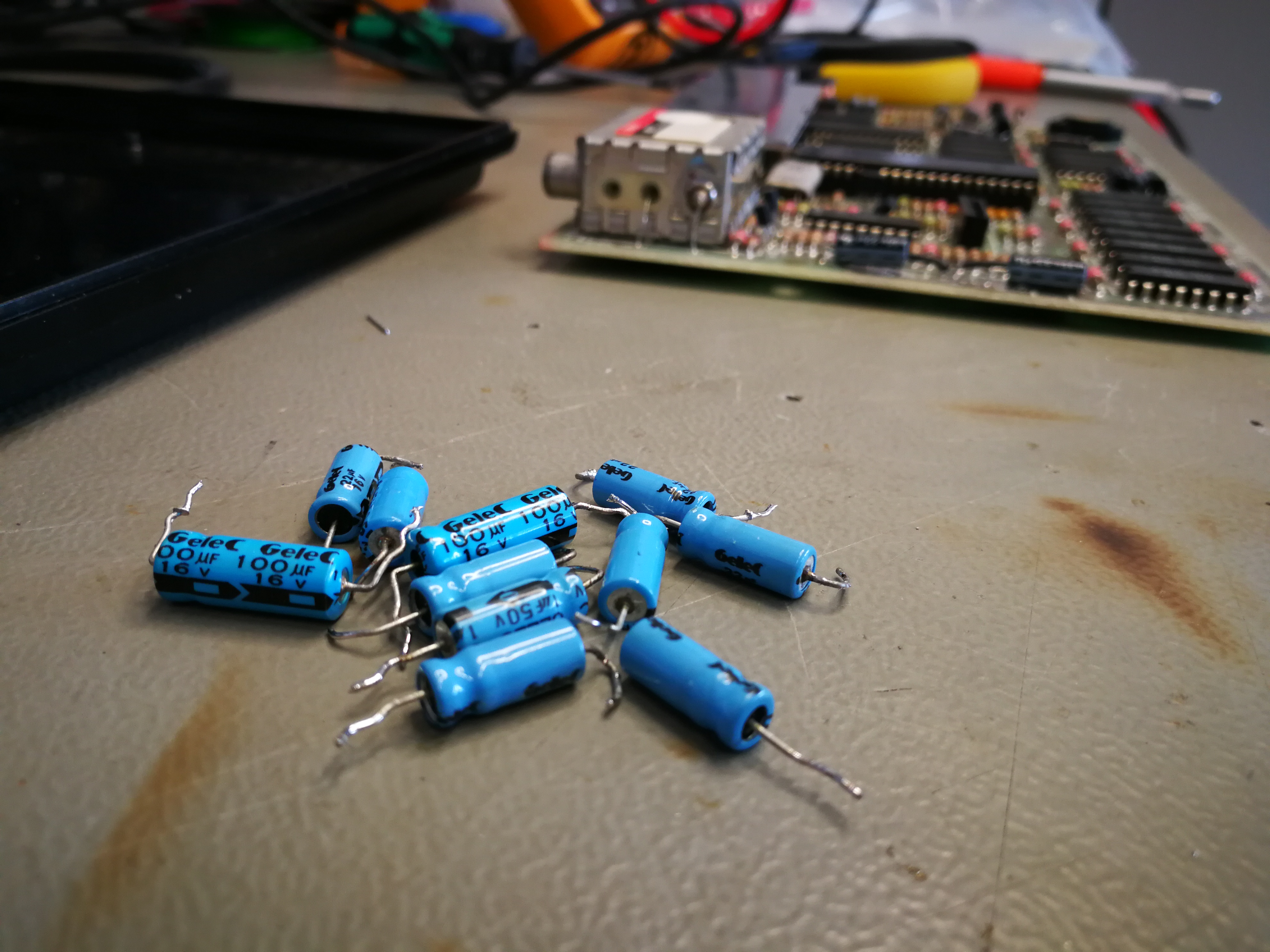
In the next step, the over 30 years old axial electrolytic capacitors are exchanged. This is a pure precaution, because as everyone knows, these parts like to change their values with increasing aging or run out. And what leaked electrolytes can do so everything, I have already shown in older posts. In order to allow the ZX a longer life again, all Elkos are exchanged.
die alten Elkos
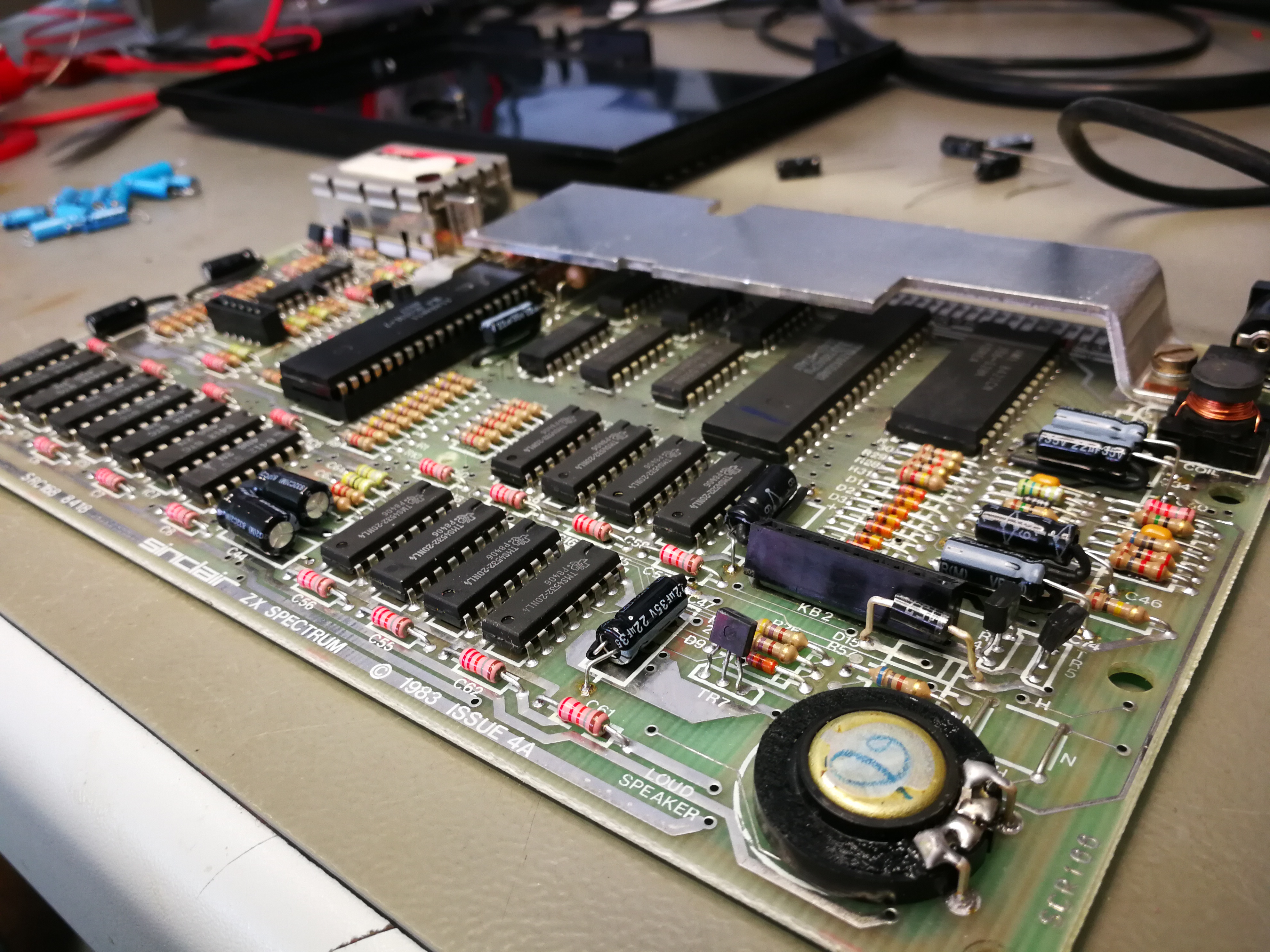
Mainboard mit neuen radialen Elkos
Once this work is done, then the exciting part begins. The power supply is switched on. It is best to supply the ZX with a laboratory power supply with adjustable current limit. He may take after switching on not more than 750mA at 9VDC. If that also fits, the voltages can be measured (best on one of the lower RAM ICs). It should be measured at PIN1 -5V, at PIN9 + 5V and at PIN8 12V.
Conversion of the RF modulator to video output
In order to be able to connect the ZX-Spectrum to a display unit, there is the RF modulator, which modulates the internally generated composite video signal onto a UHF channel carrier in order to operate a classic analogue TV. Since television receivers with analogue tuner are now hardly available anymore, but many TV have at least a SCART or video input, the RF modulator of the ZX-deactivated. The former antenna socket is converted into a video output. First, the two wires coming out of the modulator are unsoldered from the motherboard. (These are + 5V and CVBS). Then inside the modulator, the pin of the resistor is unsoldered from the inner conductor of the antenna socket and bent away. Thus, the modulator is completely disconnected from the circuit. Now only the CVBS output from the motherboard needs to be soldered via a capacitor to the inner pin of the socket. The capacitor should be around 100uF. It serves as DC decoupling of the signal.
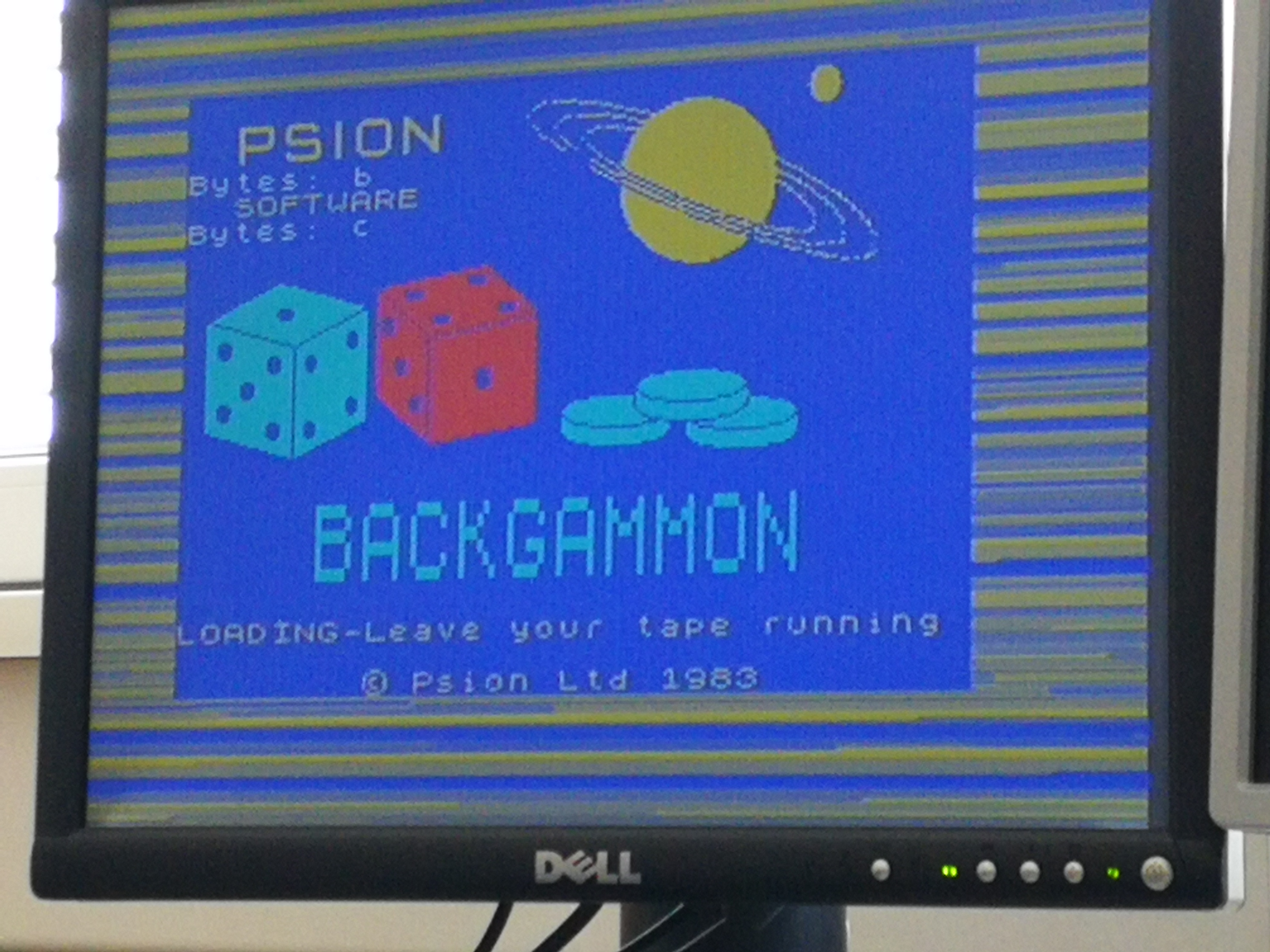
When all this is done, you can now connect and power up. In my case, it was a complete success. The Sinclair reported immediately with its gray-screened startup screen “(c) 1982 Sinclair Research Ltd” Next, I tried an old original game (backgammon) on the tape recorder (data recorder) to load into the ZX. That did not work for the time being. Sometimes a part was loaded, then again not and it came to “Tape Error” messages. So the tape recorder was also quickly overtaken. A new belt made for a better synchronization of the band and a head cleaning for nicer levels of the output signal. But even now the shop did not work. (this reminded me strongly of the time, where often a long time was trying to load a game) So I saw with the Oszi the output signal and especially the period of the initial signal (the first whistle on the band :))
Einstellung der Bandgeschwindigkeit
Here it was, the problem. The frequency of the initial signal was about 890-910Hz. That means the tape runs way too fast. The problem is resolved quickly. Almost every cartridge drive has a small potentiometer to adjust the tape speed of the servo drive. Even so in this case. The frequency should be around 800Hz. The result was then:
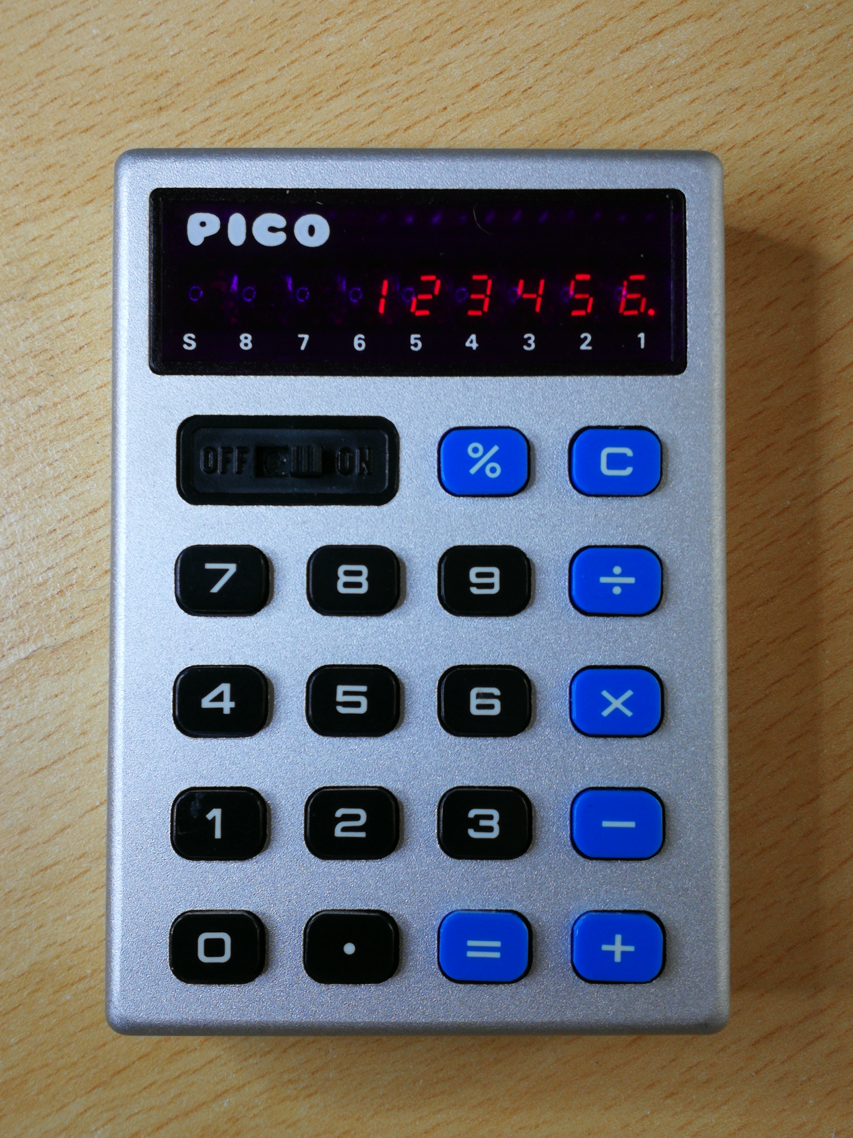
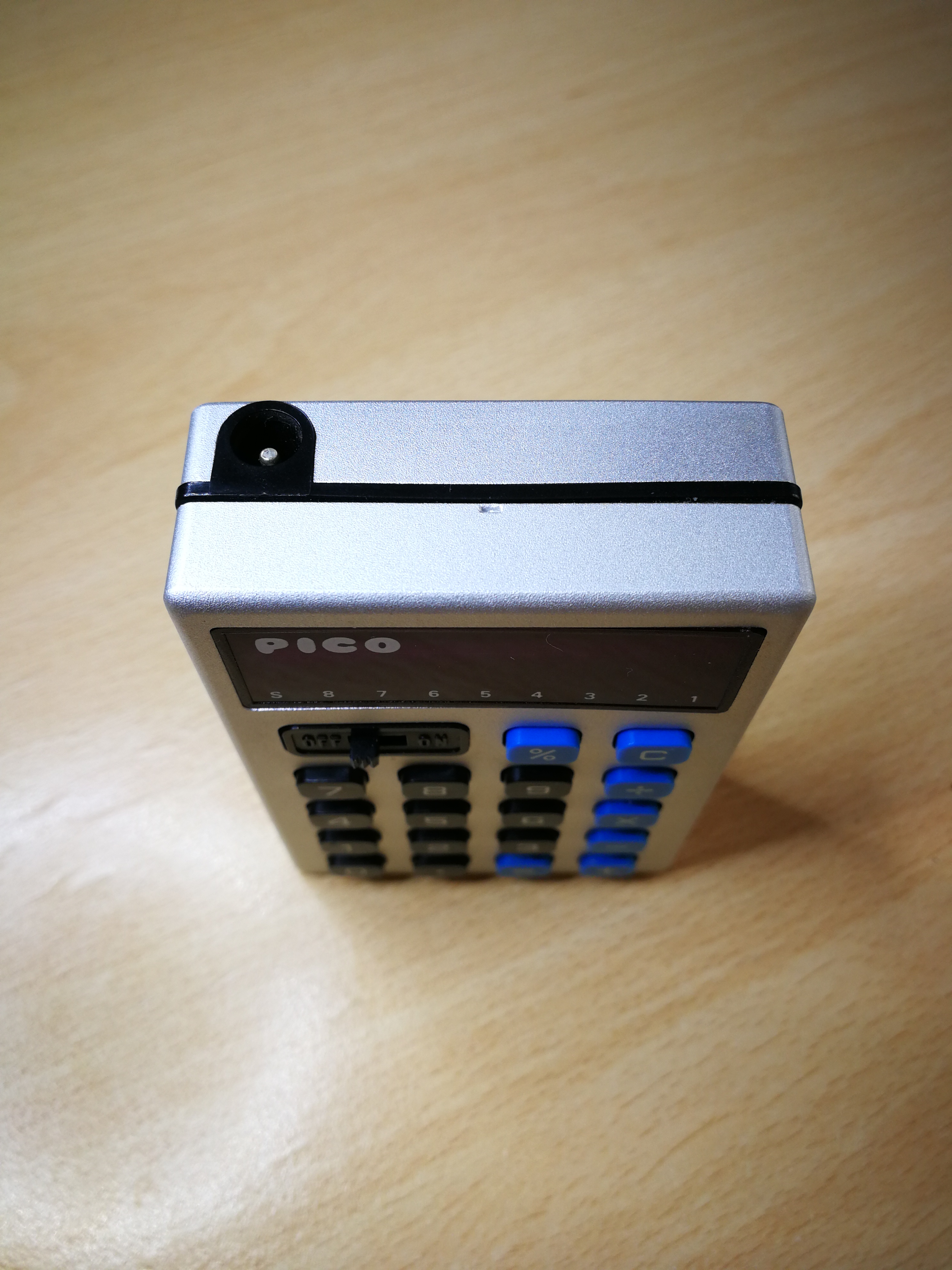
From 1975 this Japanese calculator comes. He was sold from 1975 to 1976 by the Eduscho – Tchibo coffee chain. The device is called “PICO” PA-80N. Exactly this model was also once in my father’s possession and I was already fascinated by the luminous seven-segment displays as a child. And that was the problem again. As far as I can remember, I was in elementary school age, when I first disassembled the device into its individual parts. That was not the problem, but it was not there. Over time, I disassembled the computer several times. At some point wires broke off and nothing worked. Reassembled, the Pico then disappeared into a box and was disposed of years later by my father. Why I took apart and assembled the small computer again and again, I can not say today anymore. Apparently it was the success of an eight-year-old, after assembly again to have a working device – just to last. 🙂 On an online flea market platform, I found just such a calculator and in addition to that in a TOP condition and almost gave it. So I had to have him …
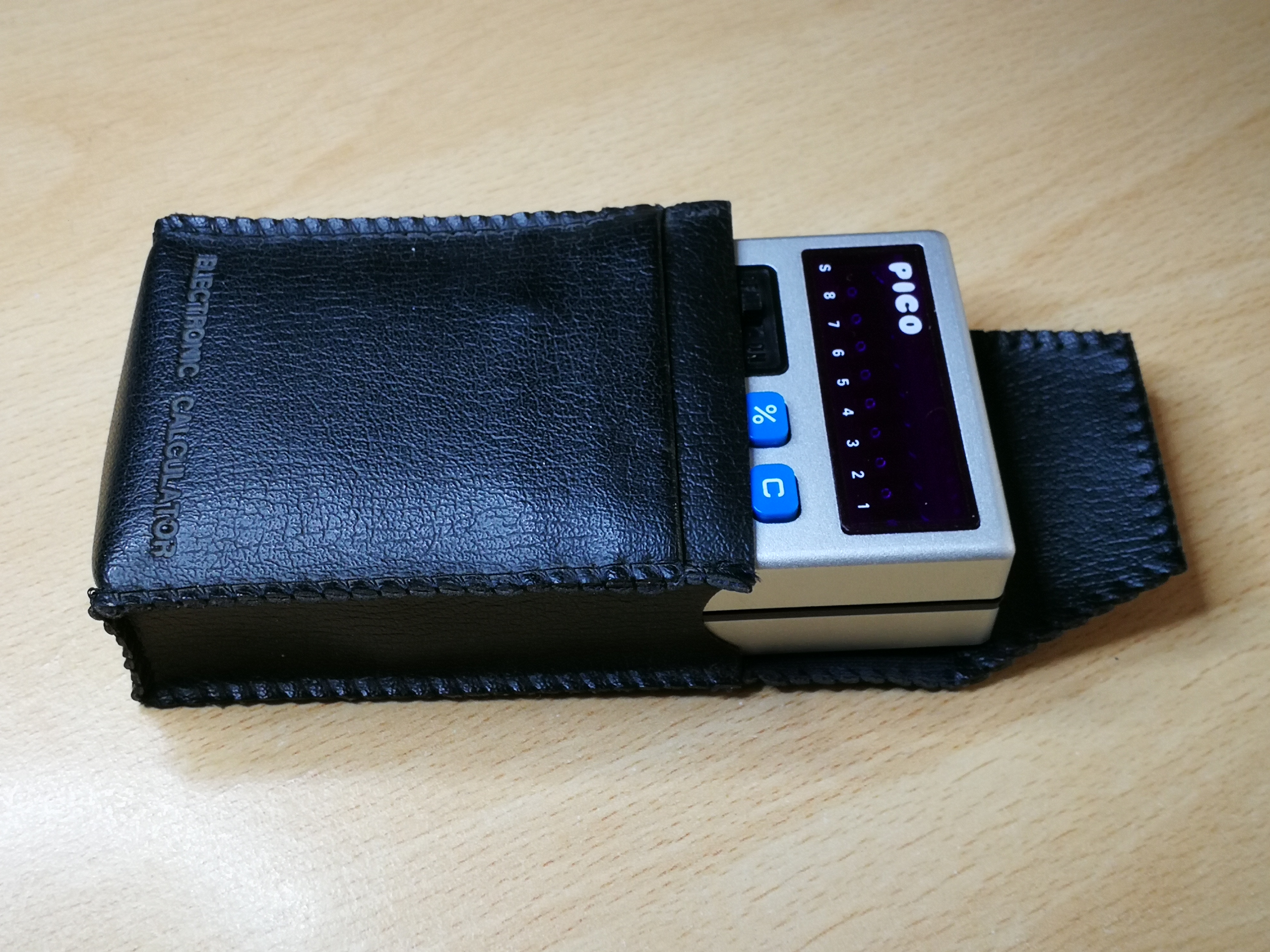
Pico with the imitation leather case
To the dates:
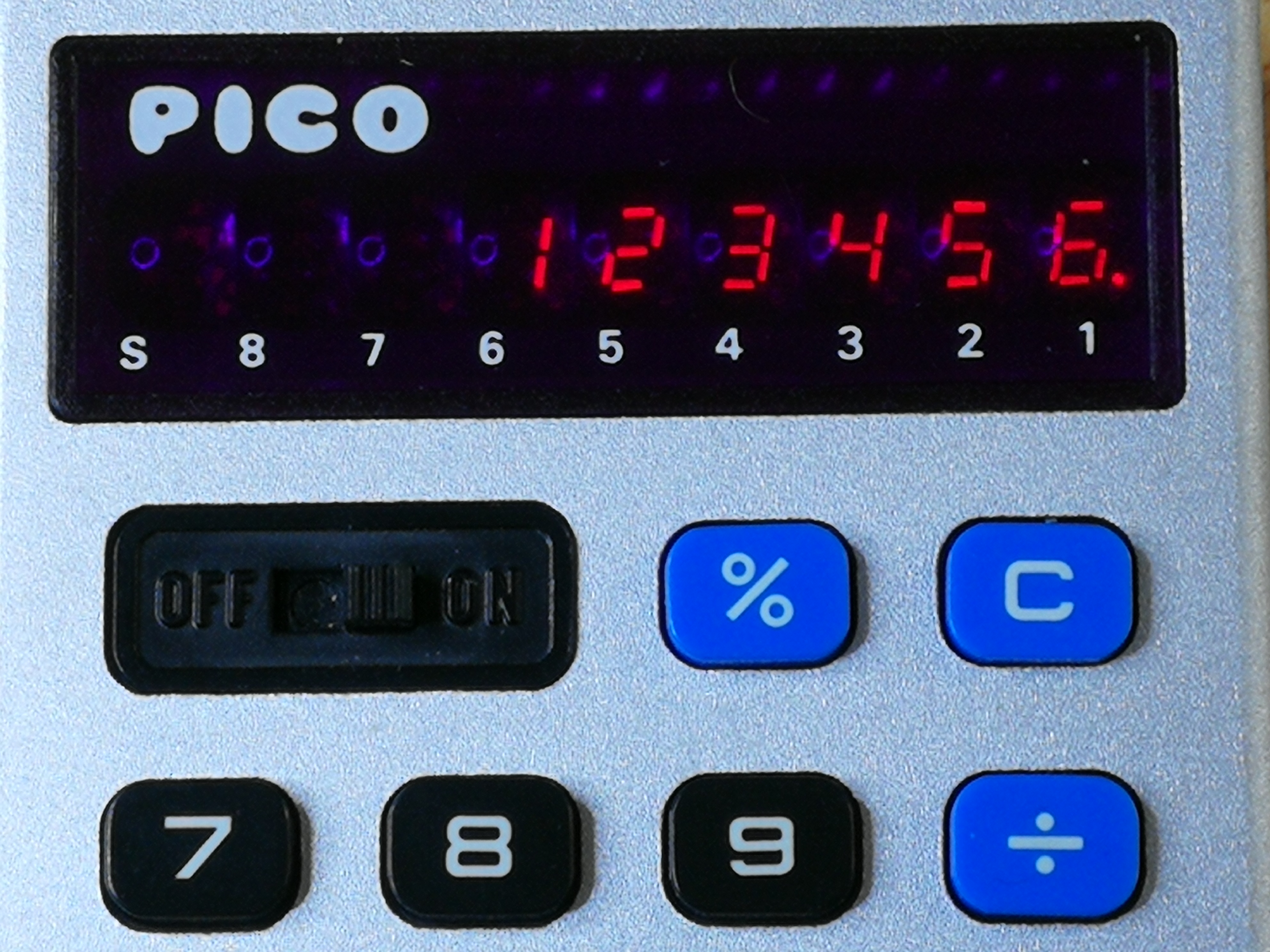
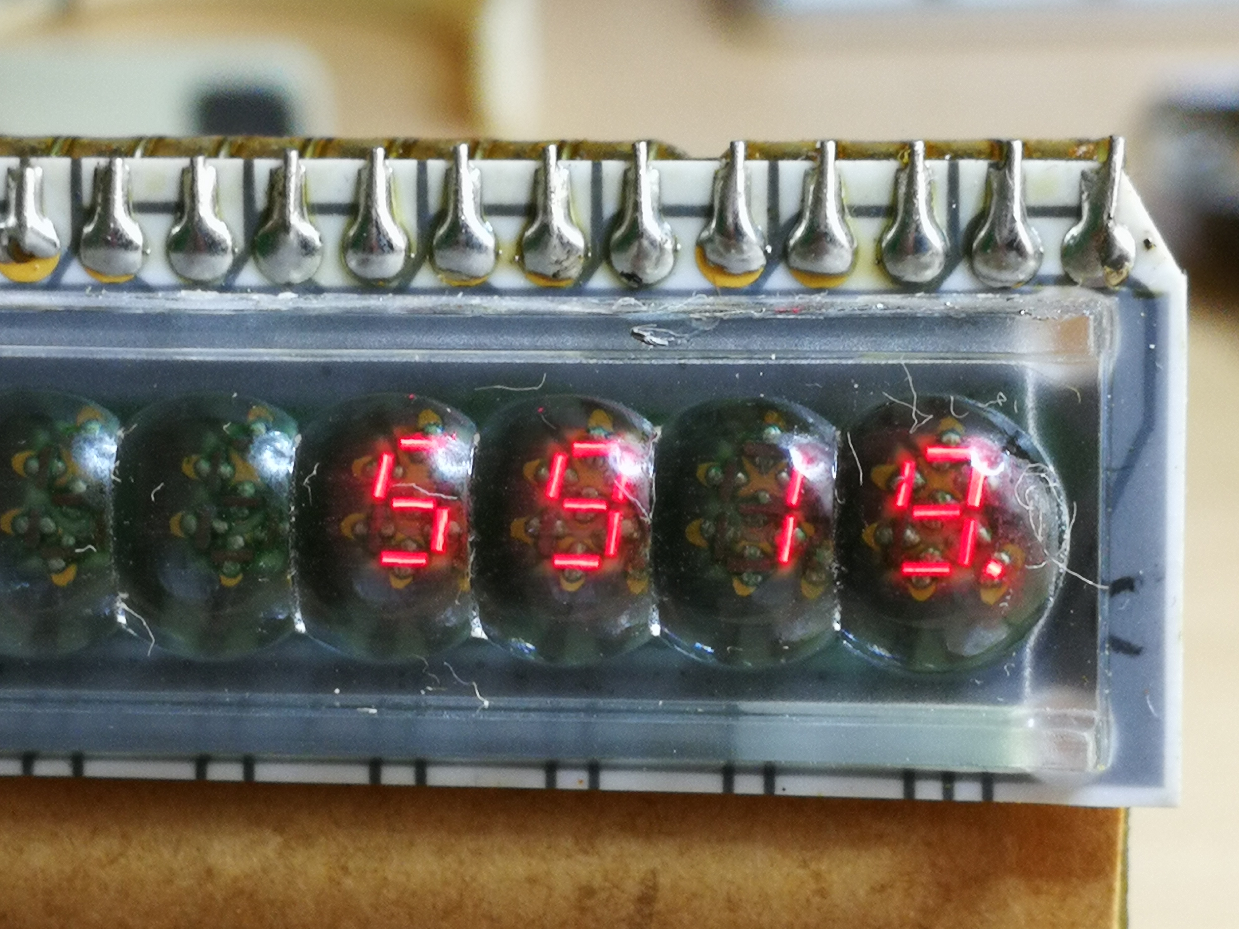
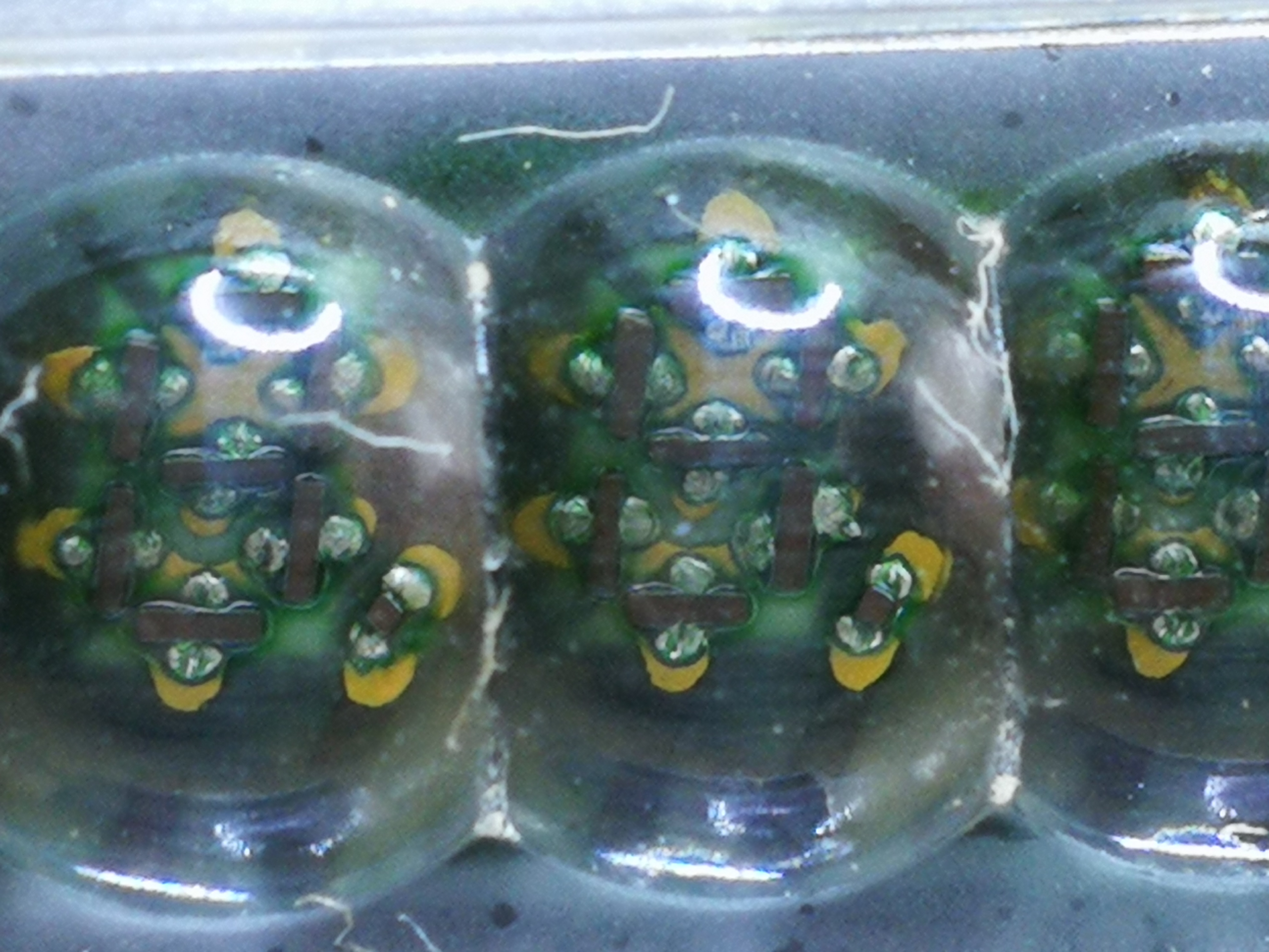
The display has eight 7-segment digits based on LED technology. To be able to read the MikroLEDs they are embedded in a convex shaped plastic. This achieves a magnifying effect that makes the numbers readable.
Siebensegment – Anzeige mit 8 Digits
LEDs under the convex plastic encapsulant
The housing is made of aluminum and plastic and has the dimensions in about a cigarette box. 8.2 x 5.7 x 2.4 cm. In order to keep the calculator gently, there was a leatherette case to do so.
Mainboard des PICO
The calculator is powered by two Tripple A (AAA) batteries, so with 3V. Optionally, there was also an external power supply that could be purchased according to the then price list by almost 18DM. (unfortunately no price information for Austria)
Power adapter socket at the top
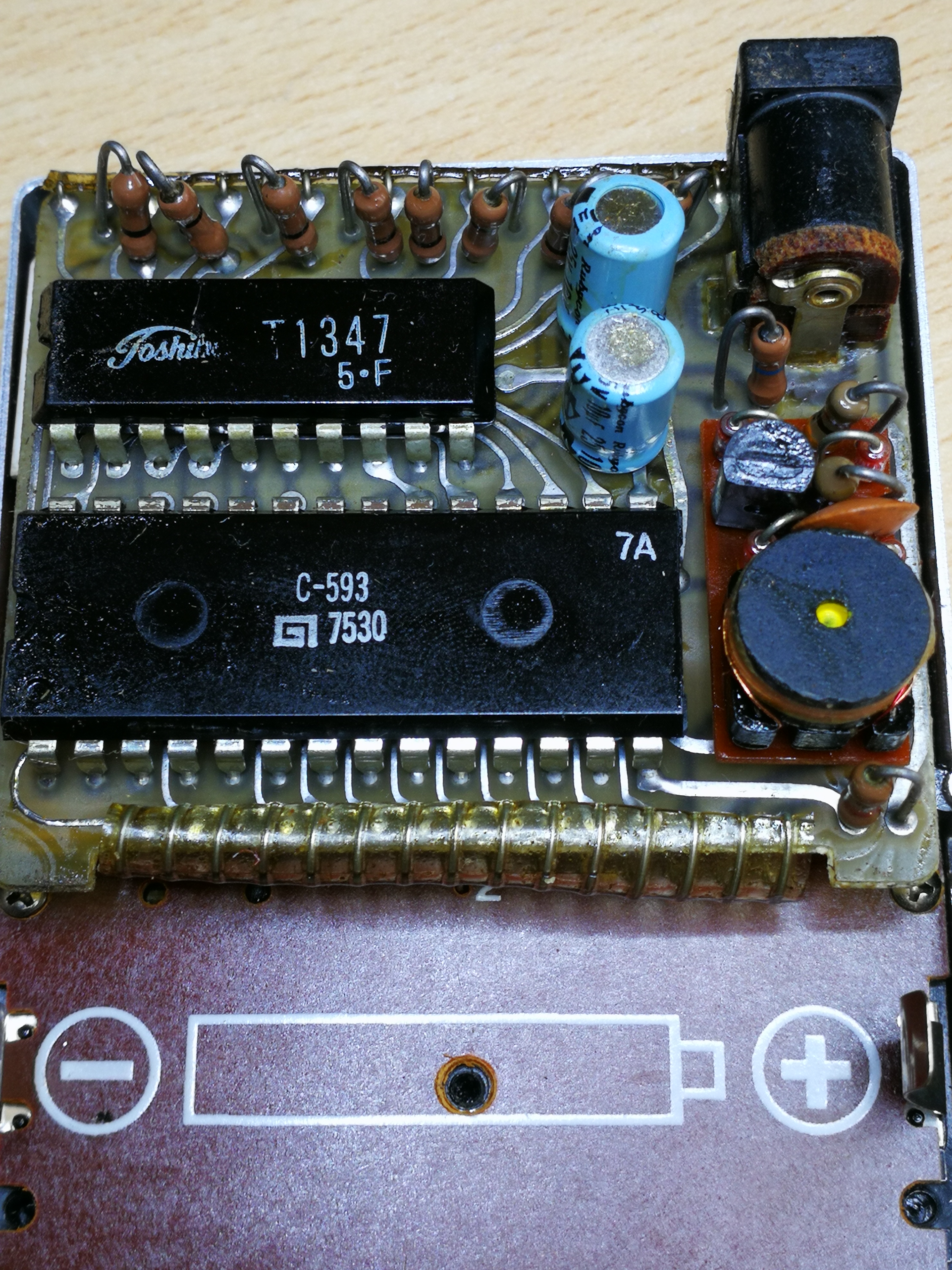
Technically, the small computer consists of a display board, a “motherboard” and a keyboard board. These boards are connected to each other with a multipolar bridge line. This should not be bent too often, because then quickly break off individual wires …
Opened circuit boards
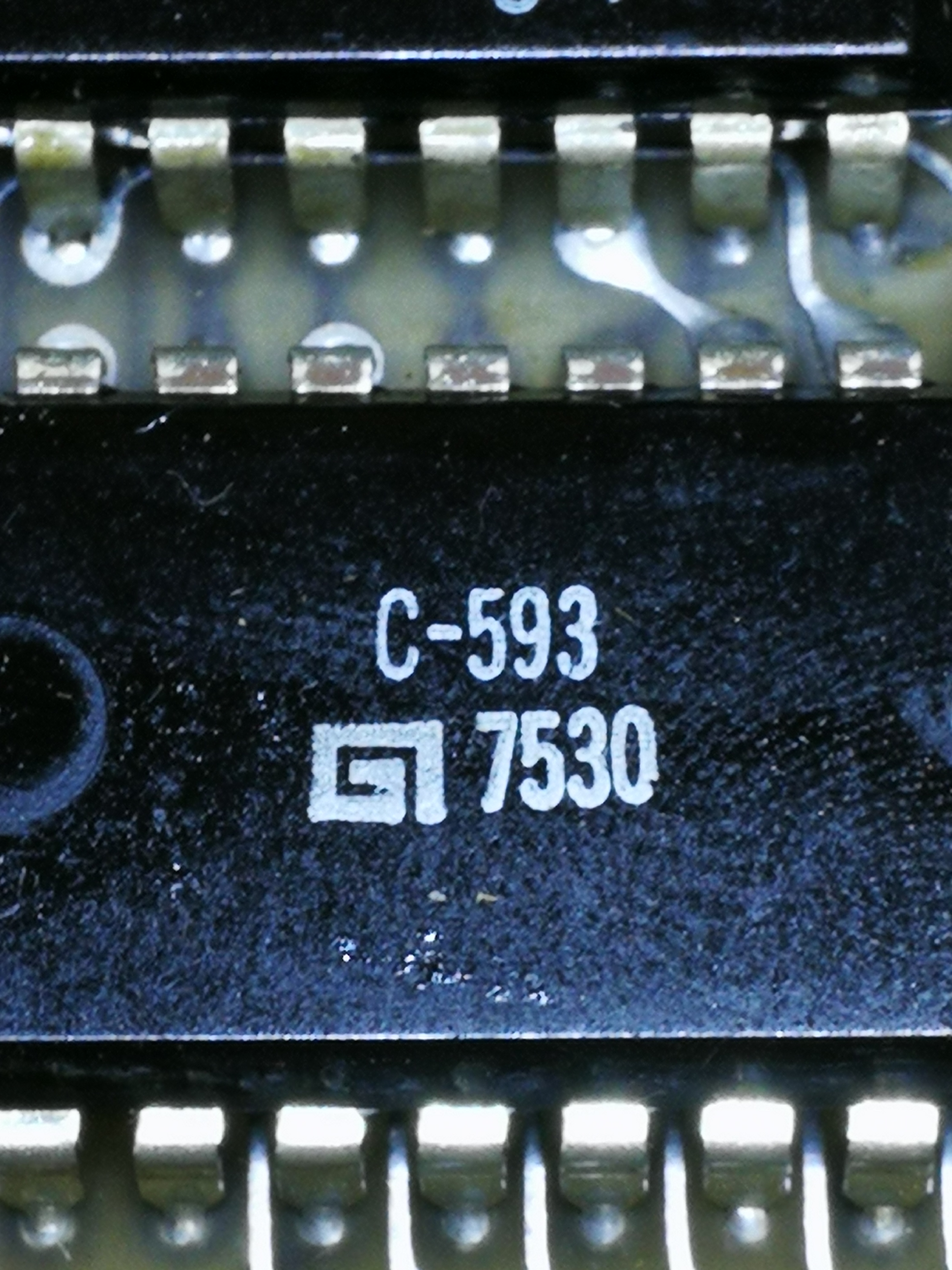
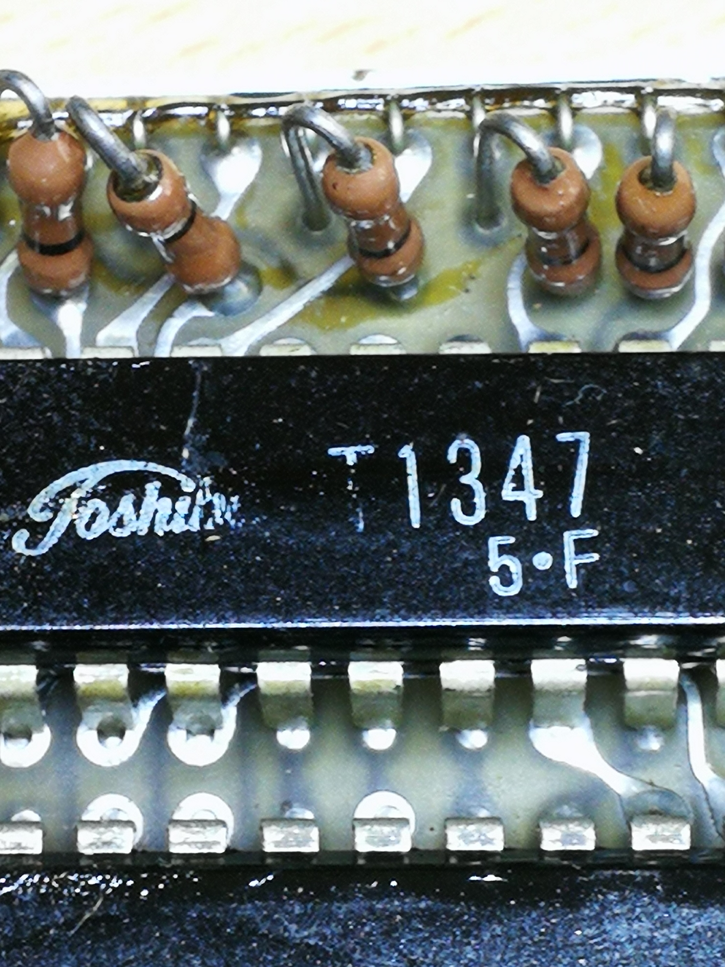
The display board is driven by a Toshiba T1337 Displaydriver IC and the computer itself is a GI C593 (General Instruments) processor that handles the basic operations and percentage calculation. The processor works with a supply voltage of 15-17VDC and is able to drive Floureszentplays directly. In order to produce in the small Pico computer from the 3V of the AAA batteries also the 17VDC a small DC / DC converter on the Mainboard expires.
central processing unit
displaydriver
DC / DC converter circuit for the 17V of the CPU
datasheet from theC593 (source: 1977 Datacatalog GI Microelectronics)
In addition to the faux leather case, there was also a card with a user manual and a flyer. It was printed with warranty information and an advertising slogan:
“The Pico will become an indispensable arithmetic assistant for you. At school, at home, at work – wherever there is something to be expected, the Pico is at your fingertips. Just press keys, and you’ve already calculated the most complicated tasks. This is how arithmetic becomes a pleasure! “(Source: Internet)
Unfortunately, the intervals in which I find some time to write a new post for the blog have not gotten shorter. But post a post per month, I think … 🙂
This time it’s not a retro craft project from the local Gefielden or a restoration of an old device, but again something about Arduino. The idea – to build a sensor that, as always, transforms a physical quantity into an electrical signal. This is nothing special and what kind of sensor it will be, I will not describe for the time being. But there should not be a sensor board, but many. And these sensor boards short “sensors” are to be networked together in a two-dimensional matrix. You can imagine it as a chessboard, with each of the chessboard panels representing a sensor. This network of sensors – ie sensor nodes – should then be connected via a transfer point to a computer and output the sensor data of the respective field. It should then also be possible to remove individual fields from the network without the remaining network losing its function.
The whole system should be as simple and cheap as possible. And so a system concept was quickly developed in which the nodes communicate via the I²C bus and send their data to a master. The following diagram is intended to illustrate this.
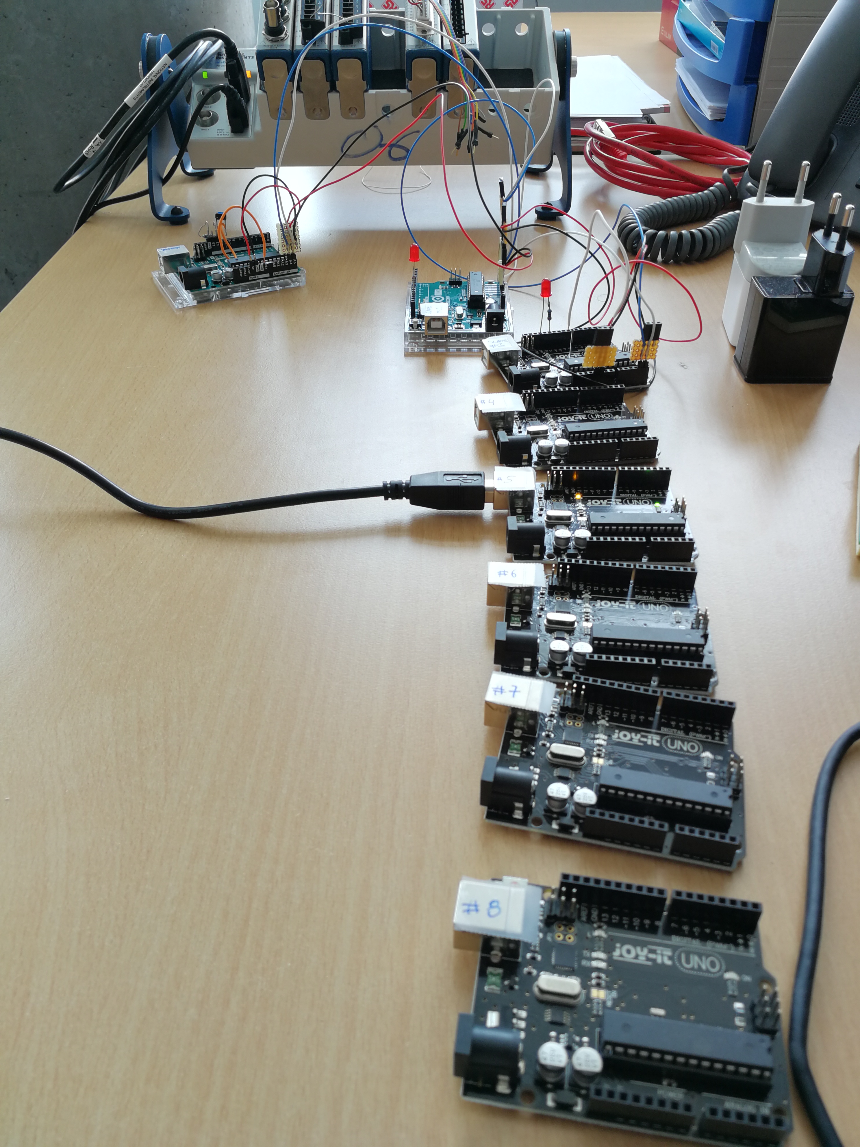
This concept, I thought, is easiest to implement with an ATmega microcontroller. The has enough IO’s, an I²C bus and UART onboard, as well as analog inputs and requires little component peripherals to bring it to life in its own layout. And there is nothing faster to do such a test setup of such a node network than to use the well-known Arduino development boards. I have chosen the cheapest version for a test setup -> the Chinanachbau of the ArduinoUno (Joy-IT UNO) with the Atmga328 in the capped DIL housing.
Joy-It Uno Boards
The picture shows ten of these microcontroller boards. Of these, one should be used as a bus master and nine as slaves. Of course, each of these slaves has a unique bus address, which only occurs once in the system. In the test setup, this bus address is permanently assigned via the program code, since anyway each Arduino must be connected to the computer in order to carry out the program upload. Of course, that should look different later. Because the Arduino is on the Atmega328 chip, its quartz and the few resistors reduced on the sensor board with gelayoutet. The chip should then be programmed via the ISP pins. Of course, as many boards do not always customize the program code and they all have the same Flash file, I want to set the sensor address with a 7-bit DIP switch. A 4021 Cmos Static Shift Register is supposed to read the bits after the controller is powered on and push them serially into the controller. The resulting value is then available as a bus address in a variable.
Each of these slaves with their individual bus address is now queried in sequence by the master node, which state it has and whether it should switch an output or not. That is, the node has only one DO (digital output) with which it can, for example, turn an LED off and on and interrogate one or more DIs (digital input) which polls a state, for example a simple switch. These functions are stored in 2 bits of a byte. Another byte is used to transfer the bus address. So two bytes are sent over the bus. The picture below shows the test setup with the “UNO boards”
All Arduinos are connected to I²C data bus and power supply
The process is as follows:
MASTER: The master node sends a request after the series to all slave addresses and a switch command (which comes from all nodes of a TEST push button input on the master) for the LED output of the node and sees if a response comes back or not. If no answer comes, the node is not in the network or is defective. If there is an answer, this consists of the address of the node and its status byte. This information is transmitted via an RS232 terminal to the computer connected to the master. Thus, for example, the switching status of each individual node can be displayed on the screen via a visualization using (NI LabView, or Matlab or similar). By adapting the master program, it is also possible to switch the LED outputs of the slaves via the computer.
SLAVE:
When the master node requests data from the slave, the slave sends back two bytes. Where byte0 again is the slave ID (ie bus address) and byte1 is the data. Byte1 actually consists of only two bits encoded as follows (in decimal representation):
0 = LED off| Sensor not triggered
1 = LED on | Sensor not triggered
2 = LED off | Sensor triggered
3 = LED on | Sensor triggered
// I2C Slave Code// 16.05.2018 // ver 1.3#include <Wire.h>#define ADDRESS 2 // adresse des slave knotens#define PAYLOAD_SIZE 2 // anzahl der bytes die vom masterknoten zu erwarten sindint LED=12; // indicator led an pin D12int SENSOR =8; // sensor input an pin D8bool actionState=0; // sensor zustandint busstatus; // statusvariable // 0 = LED aus | sensor nicht belegt// 1 = LED ein | sensor nicht belegt// 2 = LED aus | sensor belegt// 3 = LED ein | sensor belegtbool sensled=0; // sensor LED
byte nodePayload[PAYLOAD_SIZE];
voidsetup()
{
pinMode(LED, OUTPUT); //sensorLED
pinMode(SENSOR, INPUT); //Sensor
Wire.begin(ADDRESS); // Activate I2C network
Wire.onReceive(receiveEvent);
Wire.onRequest(requestEvent); // auf master anforderung warten// // debug interface// Serial.begin(9600);
}
// *********************************mainloop****************************************************voidloop()
{
delay(5);
if(sensled){digitalWrite(LED, HIGH);}
else{digitalWrite(LED, LOW);}
actionState = digitalRead(SENSOR); //Sensoreingang abfragen if((actionState==1)&&(sensled==1)) {busstatus=3;}
elseif ((actionState==0)&&(sensled==1)) {busstatus=1;}
elseif ((actionState==1)&&(sensled==0)) {busstatus=2;}
elseif ((actionState==0)&&(sensled==0)) {busstatus=0;}
// Serial.println("######################");// Serial.print("busstatus neu setzen ");// Serial.println(busstatus);// Serial.print("sensled LED ");// Serial.println(sensled);// Serial.print("actionState ");// Serial.println(actionState);// Serial.println("######################");
nodePayload[0] = ADDRESS; // Adresse in byte0 zurücksenden.
nodePayload[1] = busstatus; //byte 1 ist die statusinfo der LED
}
// *********************************************************************************************voidrequestEvent()
{ Wire.write(nodePayload,PAYLOAD_SIZE);
Serial.println("bytes status schreiben");
Serial.println(nodePayload[0]);
Serial.println(nodePayload[1]);
delay(5);
}
// *********************************************************************************************voidreceiveEvent(int bytes) //einen wert vom I2C lesen
{
busstatus = Wire.read(); //If the value received was true turn the led on, otherwise turn it off // Serial.println("status empfangen");// Serial.println(busstatus);if((busstatus==1)||(busstatus==3)){sensled =1;}
else{sensled =0;}
}
The bus address must still be entered individually in this slave code. In the next version, the previously described “serializer” of the parallel dip-switch variant will be implemented. The following code example is from the master node, which reads out the slaves and sends a LED pattern to the sensor slaves using the test button:
// I2C masterknoten // 16.05.2018 // ver 1.2// changes abfrage wenn kein knoten am bus dann 255 ausgeben#include <Wire.h>#define busbytes 2 // wievele byte vom I2C knoten zu erwarten sind#define maxKNOTEN 10 // anzahl der zu scannenden slaves#define startKNOTEN 2 // startadresse der slaves#define DELAY 5 // einfach ein delay ....int i; int j=0;
int buttonPin =12;
int testbut =0; int anim =0;
int buttonState =0;
int DATEN[busbytes];
int adresse; int busstatus;
byte sensorbelegt; byte ledsensoron;
// 0 = LED aus | Sensor nicht belegt// 1 = LED ein | Sensor nicht belegt// 2 = LED aus | Sensor belegt// 3 = LED ein | Sensor belegtint leddat1[] = {1,1,1,1,0,1,1,1,1}; // -int leddat2[] = {0,0,0,0,1,0,0,0,0}; // |voidsetup()
{
Serial.begin(9600);
Serial.println("MASTER-KNOTEN");
Serial.print("Maximum Slaveknoten: ");
Serial.println(maxKNOTEN);
Serial.print("Datengroesse in byte: ");
Serial.println(busbytes);
Serial.println("***********************");
Wire.begin(); // Activate I2C link
pinMode(buttonPin, INPUT); // test-tastereingang festlegen
}
//#####################################################################################################voidloop()
{
for (int Knotenadresse = startKNOTEN; //alle knoten scannen
Knotenadresse <= maxKNOTEN;
Knotenadresse++)
//################################################################################################
{
// testbut = 0;
anim =0;
Wire.requestFrom(Knotenadresse, busbytes); // daten vom jeweiligen knoten anfordern
DATEN[0]=255; DATEN[1]=255; // wenn kein knoten dann auf 255 setzen if(Wire.available() == busbytes) { // wenn knoten und daten dannfor (i =0; i < busbytes; i++) DATEN[i] = Wire.read(); // daten holen (zuerst busID, dann daten)// for (j = 0; j < busbytes; j++) Serial.println(DATEN[j]); // daten an rs232 ausgeben
}
// Serial.println(Knotenadresse);// Serial.println(DATEN[0]);// Serial.println(DATEN[1]);// Serial.println(" ");
adresse=DATEN[0];
busstatus=DATEN[1];
if(busstatus ==0) {sensorbelegt=false; ledsensoron=false;}
elseif (busstatus ==1) {sensorbelegt=false; ledsensoron=true;}
elseif (busstatus ==2) {sensorbelegt=true; ledsensoron=false;}
elseif (busstatus ==3) {sensorbelegt=true; ledsensoron=true;}
//################################################################################################//Testbutton Status lesen und variable testbut entsprechend setzen
buttonState = digitalRead(buttonPin); //tastereingang einlesenif(buttonState == HIGH){ //wenn taster aktiv dann variable anim setzen
anim =1;
//delay(5);
}
// //debug debuginfo tasterstatus auf rs232 ausgeben// Serial.println("#######################");// Serial.print("Knoten Adresse :");// Serial.println(adresse);// Serial.print("Busstatus :");// Serial.println(busstatus);// // Serial.println("----------------");// Serial.print("Fliese belegt :");// Serial.println(sensorbelegt);// Serial.print("LED Fliese :");// Serial.println(ledsensoron);// Serial.print("#######################");// Serial.println(" ");//################################################################################################//Testbutton Status an jeweiligen knoten senden
Wire.beginTransmission(Knotenadresse); // transmit to device actual in for loop//anim schreibenif (anim==0) {testbut=leddat1[j]; j++;}
else {testbut=leddat2[j]; j++;}
if (j>8){j=0;}
Wire.write(testbut); // senden des tasterstatus
Wire.endTransmission(); // ende gelände mit uerbertragung
delay(DELAY);
}
}
With this arrangement, it is now possible to read all Arduinos and their input or to control the LED via the bus. In the next step, a “sensor” is built, a board is laid out and the ArduinoUno reduced to its microcontroller. I’ll talk about that in one of the next posts …
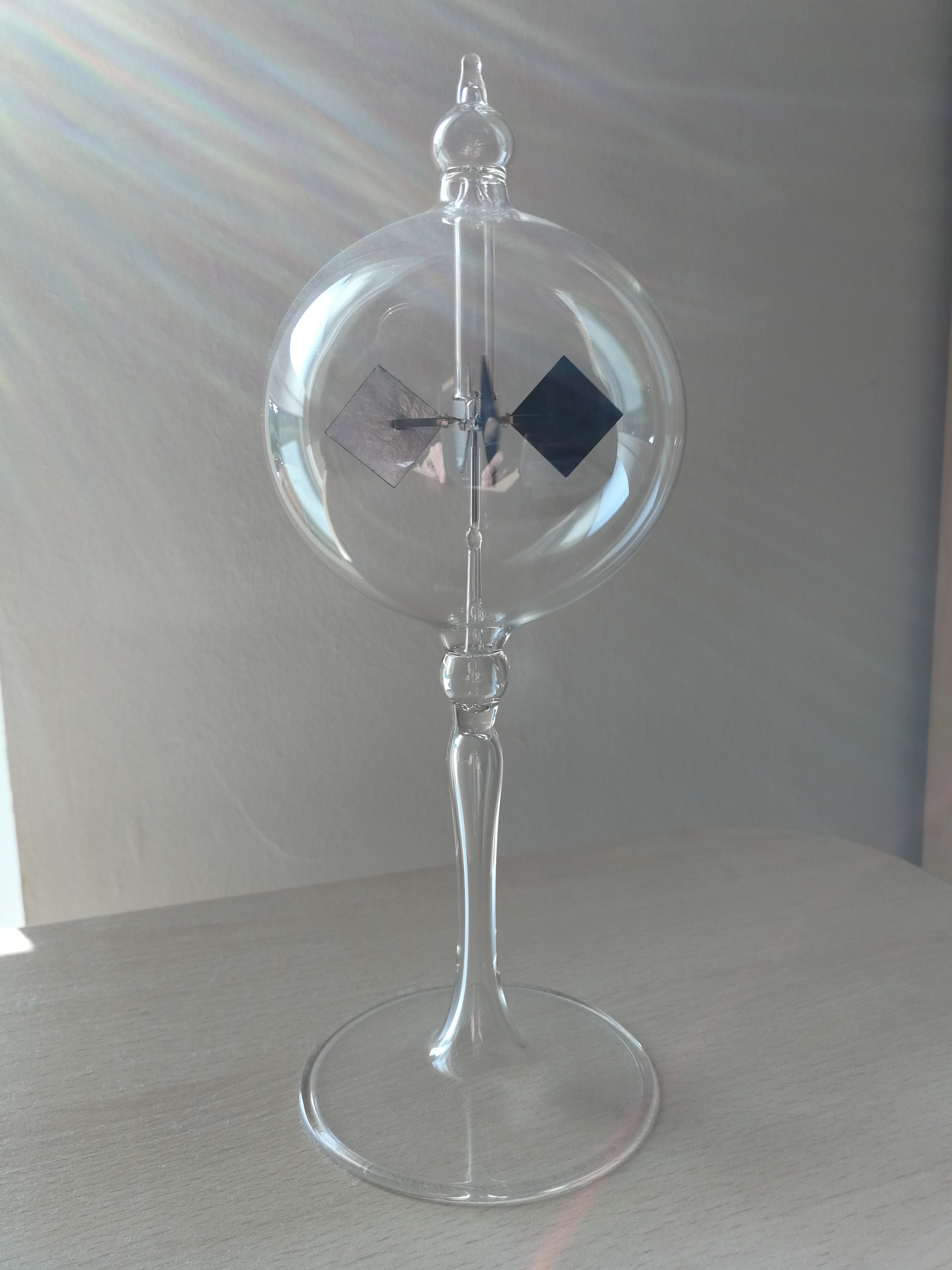
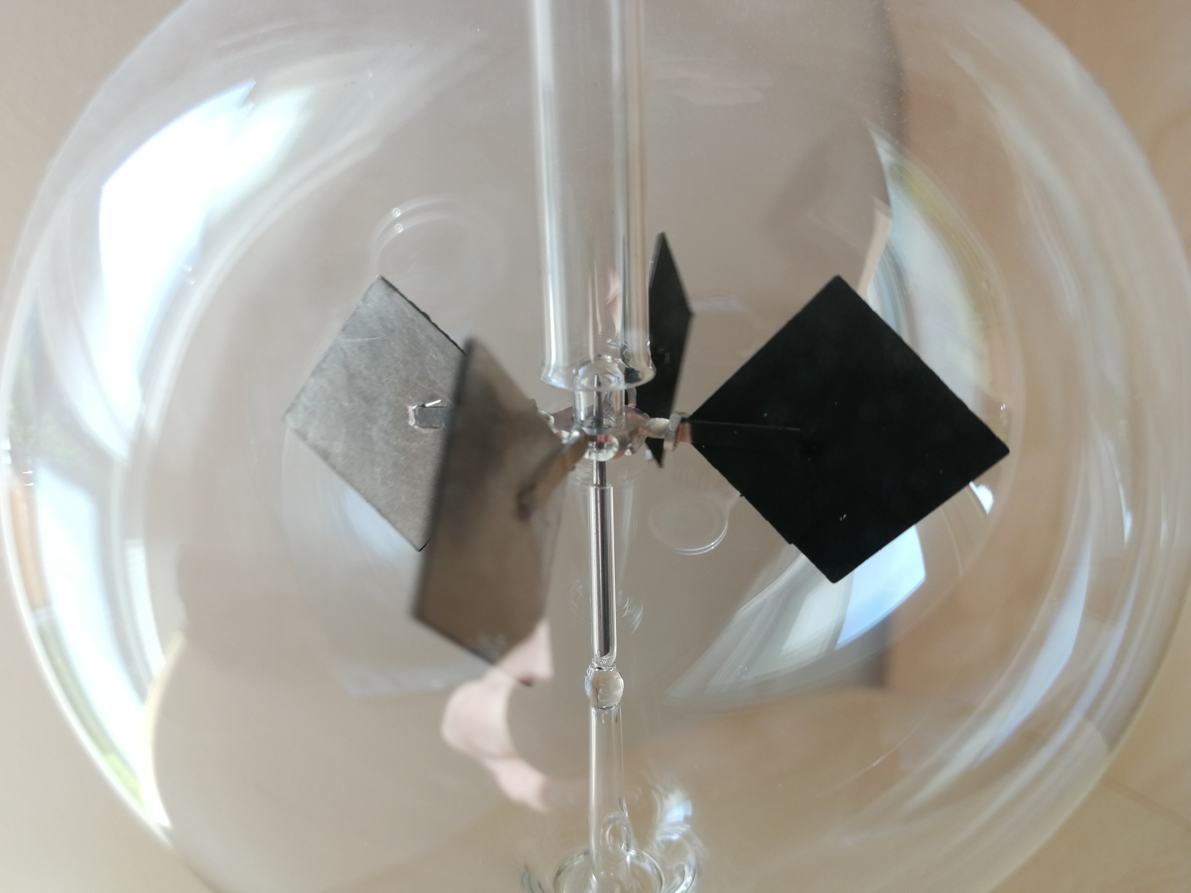
The Radiometer – also called lightmill – is an instructive, physical demonstration object that was invented about 100 years ago by the English physicist Crookes. This small physical-technical arrangement clearly shows how light is converted into mechanical energy.
The working princip of the solar radiometer:
Impeller inside the part evacuated glass ball
If warm light, ie sunlight, light of light bulbs or spotlights, meets with light in the spectrum of which the infrared component is present (but not cold light from fluorescent lamps) on the wing cross resting on a needle, this will turn depending on the intensity of the light source , In a particular method, a partial vacuum is generated in the glass ball, so that the air resistance is not stronger than the rotational force of the impeller generated by the light energy. The blackened surfaces of the wing cross absorb more light energy than the bright surfaces. Due to the warming of the air molecules, a much higher pressure is created on the dark areas than on the bright areas. This causes the constant rotation of the wing cross. (Brownian Molecular Theory). Depending on the light intensity, up to 3000 revolutions per minute should be achieved. (Source: Manufacturer of the Radiometer)
 Thanks to the USB standard, it is now easy to operate or charge your mobile phones, tablets, Arduinos, Raspberry PIs, toothbrushes, power banks, etc., etc., with one and the same charging adapter or plug-in power supply. The “plug-in power supply” is an AC / DC converter which, ideally, electrically isolates the mains side with the 240VAC / 50Hz from the low-voltage direct voltage side in compliance with the applicable regulations. The low-voltage side provides the 5VDC via a USB-A socket. Depending on the model and origin, maximum currents of 1A up to approx. 2A can be taken.
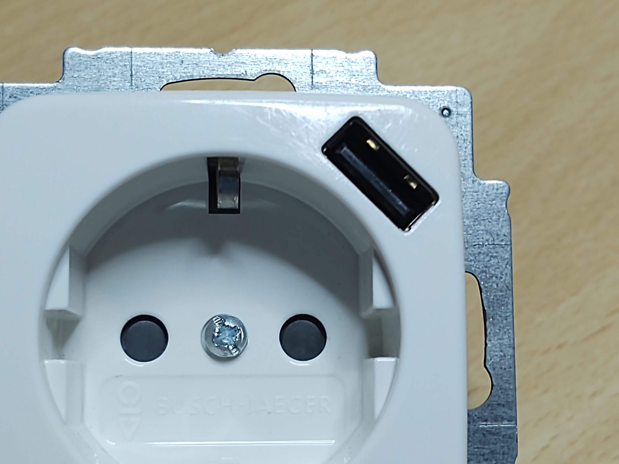


 Circuit diagram of the DC-DC converter
 Measurement of illuminance
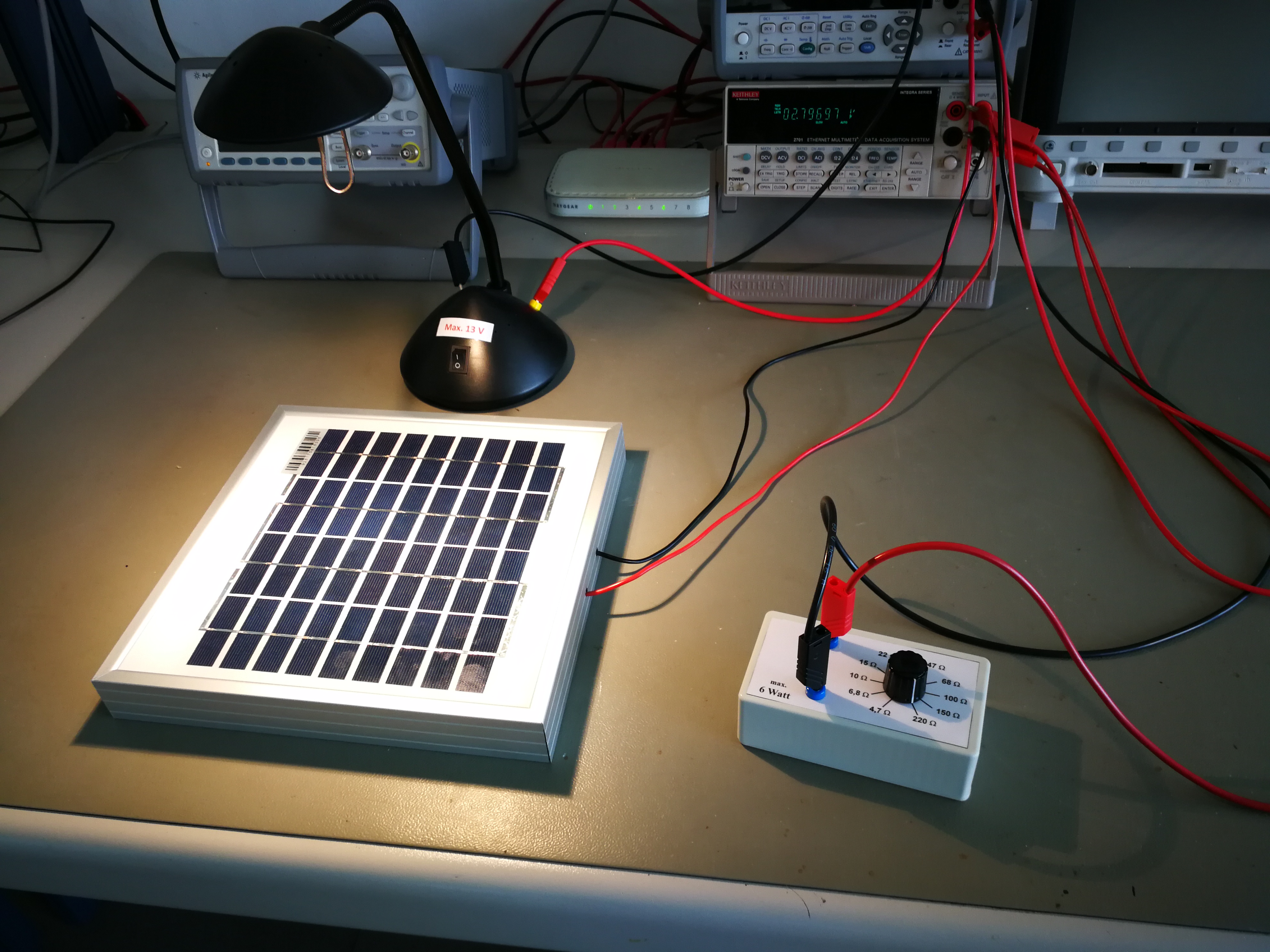 Switchable load resistors
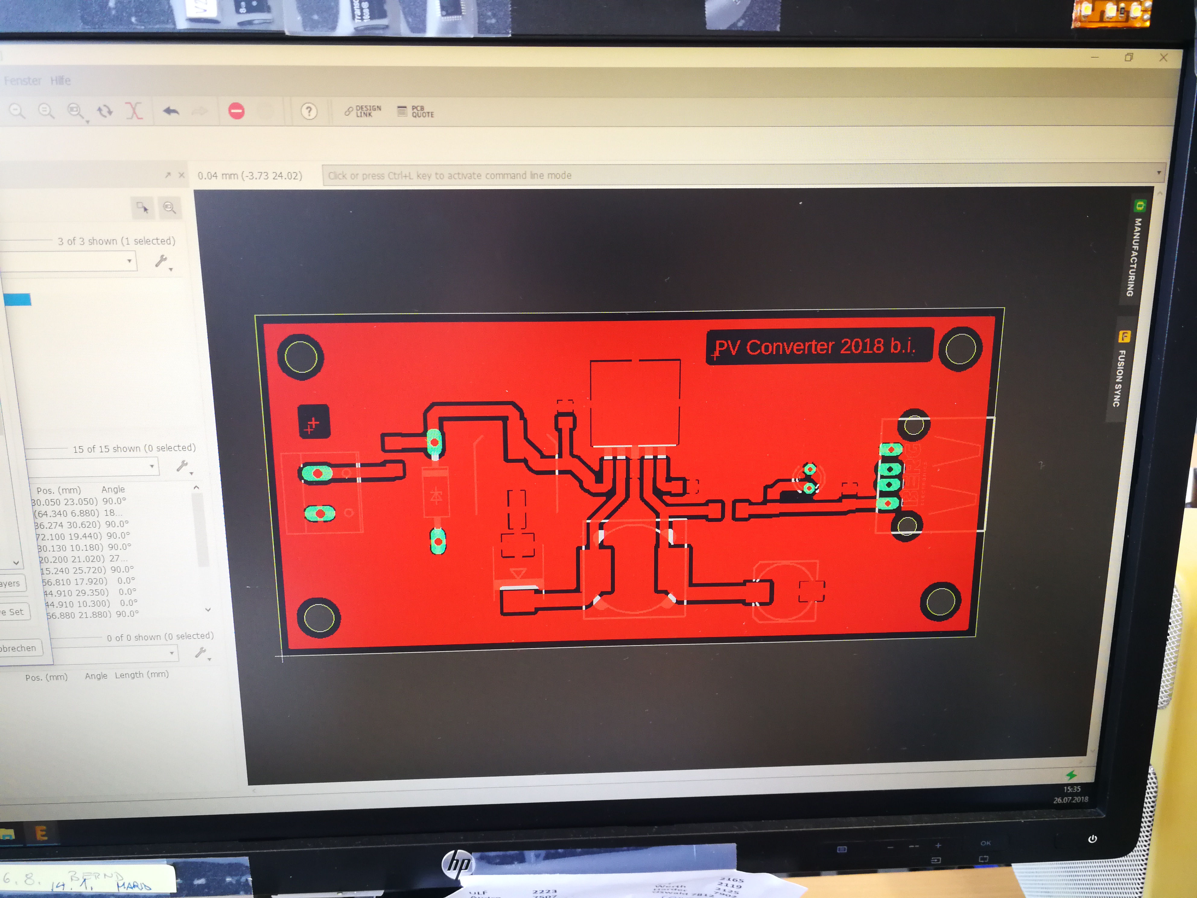 Layout on the computer
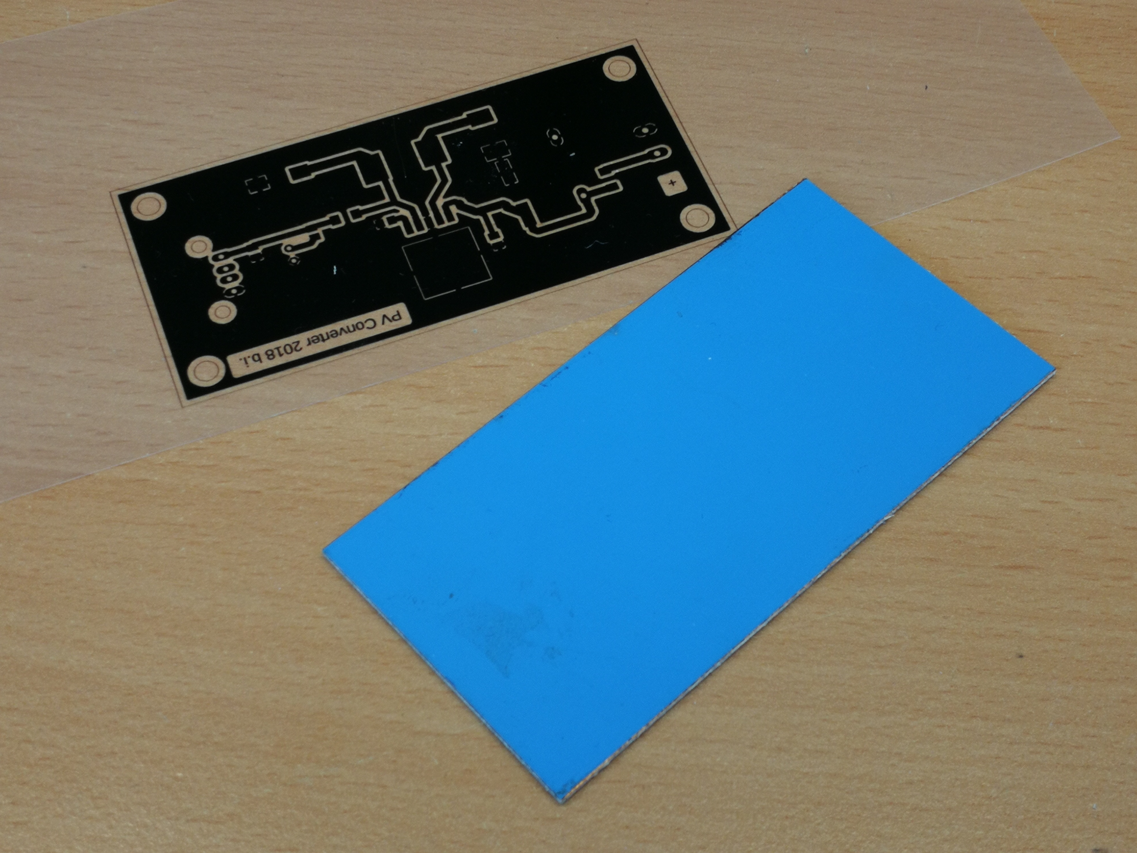 Foil for creating the printed circuit board
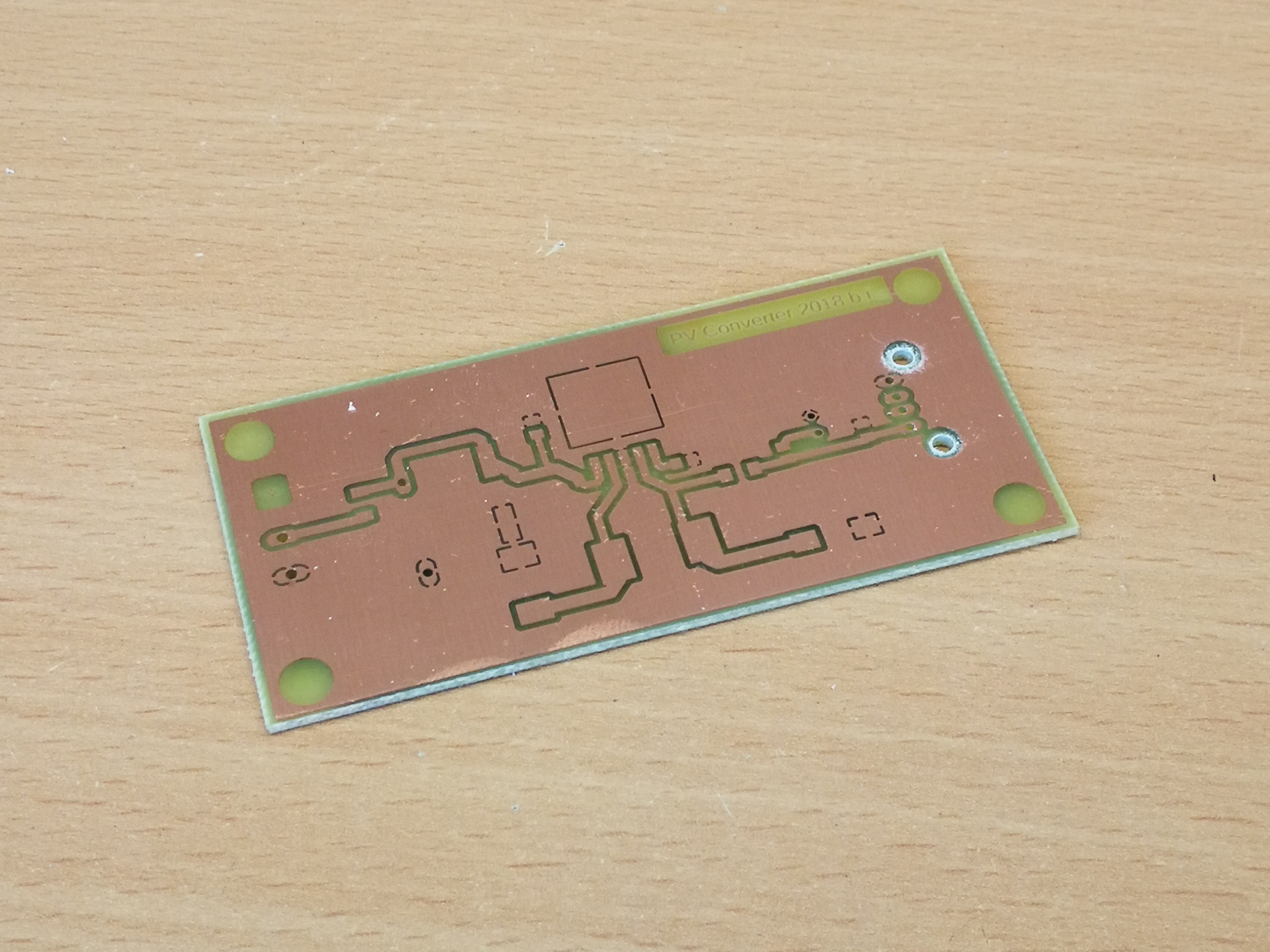 Etched PCB
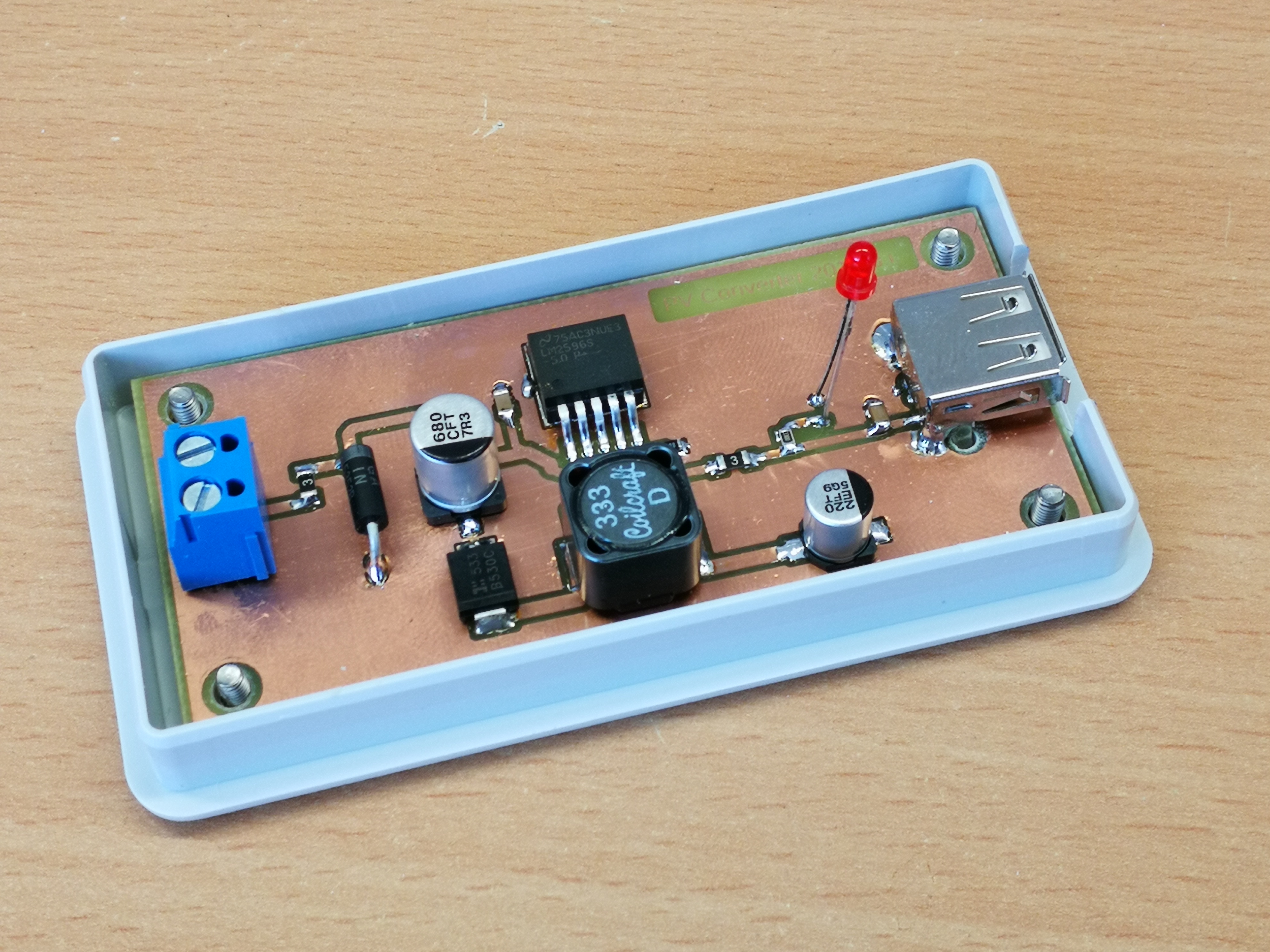 Etched PCB
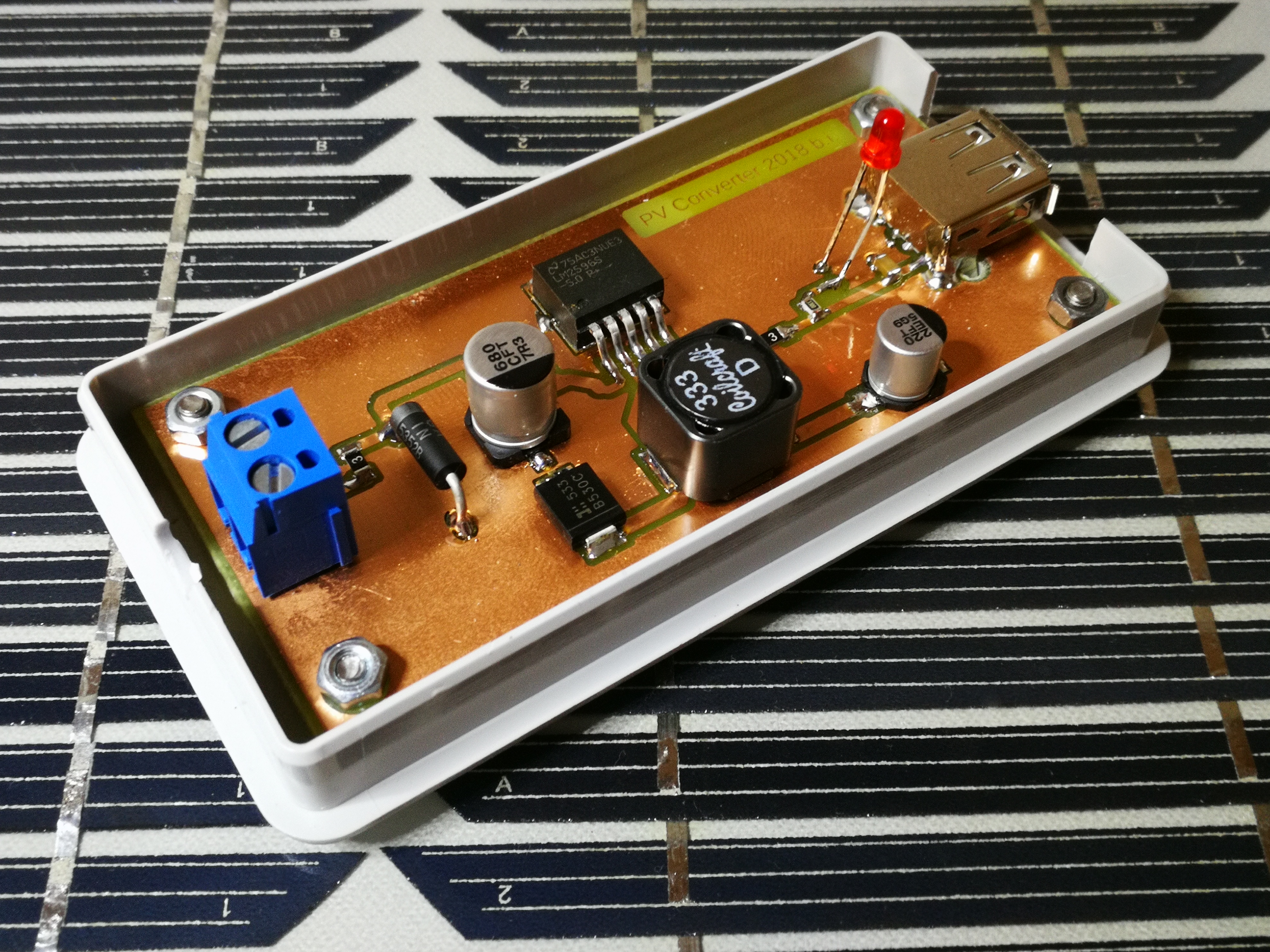 Finished circuit