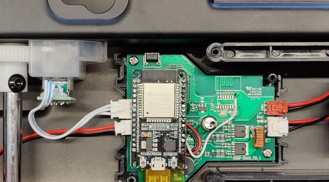
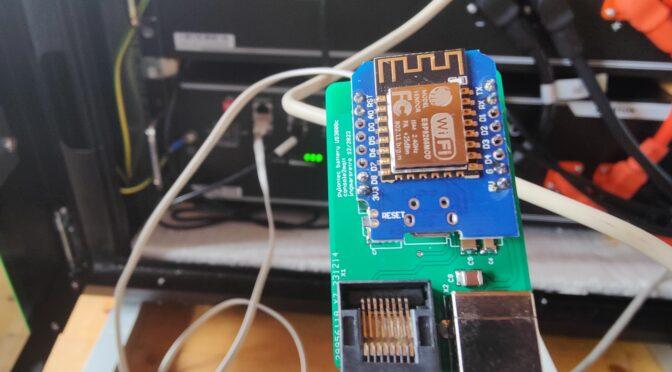
Keysight oscilloscope dies in standby – power supply repair

Loading

An interesting problem has arisen with the measurement technology in the laboratories at my workplace. I use the term “measurement technology” to describe the equipment of a laboratory workstation for basic training. There are a total of nineteen laboratory workstations, each equipped with two laboratory power supplies, two desktop multimeters, a Keysight signal generator and a Keysight (Agilent) oscilloscope of the Infiniivision DSO-X 20xx series. All devices are network-compatible and are connected to the corresponding workstation computer via LAN. This means that the measuring devices can be accessed using different software (Agilent VEE, Matlab, LabVIEW etc.). The devices were purchased around three years ago and replace the almost twenty-year-old laboratory equipment.

However, it has now happened that the DSO-X2012A oscilloscope at one workstation no longer showed any signs of life. It occasionally happens that during laboratory exercises or when working freely in the laboratories, a student presses the emergency stop switch of the workstation and thus de-energizes it. But this was not the case. All the devices connected to the workstation worked, with the exception of the DSO. Voltage could also be measured at the end of the IEC plug. So the problem could only be with the oscilloscope itself. The rear panel is quickly unscrewed, a shield plate removed and the power supply unit is exposed. The first visual inspection immediately revealed the large filter capacitor with its upwardly curved cap. But first things first.

Power supply unit of the Infiniivision

The mains voltage was measured at the AC pins of the mains input, but no DC voltage was measured at any of the outputs of the power supply unit. Regardless of whether the power switch of the device was switched on or off. This suggests that the power supply unit is defective.

Input fusing

First, the power supply unit was removed and examined, starting with the AC input side. The print fuse in the area of the mains filter was the first defective component to be noticed. It is a slow-blow 6.3A/250V fuse. As a blown fuse always has a reason to switch off, the search continued. The mains rectifiers were OK, but the 100uF / 420V electrolytic capacitor, which is used to smooth the DC voltage on the primary side, had already suffered some thermal damage and was bloated.

original electrolytic capacitor 100uF /420V /105°C

Its capacity was also no longer within the nominal range. But even that was not the direct reason for the fuse blowing. This was quickly found. A mosfet used to control the transformer was low-resistance. More precisely, it had a short circuit between all the connections.

Mosfet STP12NM50

The following picture shows the installation positions of the components. These have been replaced. The mosfet was replaced with an original type and the power supply capacitor was replaced with a 100uF / 450V / 105°C type. Although it is about five millimeters higher, it fits easily into the power supply unit.

Installation position of the capacitor and the mosfet

Two SMD resistors on the back of the power supply board were defective in the area of the gate connection of the mosfet. These were an SMD resistor of size 0805 with 5.11 Ohm and an SMD resistor of size 1206 with 2.0 kOhm. The picture below also shows the installation position.

Mounting position of defective SMD resistors

After all the components mentioned had been replaced, a first functional test was carried out. However, this was sobering, as the power supply unit was still not working. The fuse remained intact and the DC voltage on the primary side was stable. But the gate of the mosfet was not activated – unfortunately. Because now came the time-consuming part of the repair. On the power supply board, installed upright, there is another board on which several controller ICs are installed. If you follow the gate line from the Mosfet, it ends at a pin on this control board. So this must be removed.

Controller board removed

To do this, the cooling plate had to be removed first. Then it became a bit tedious, because the controller board is not connected to the main board via a pin header or plug connection, but the contact pins are laid out and milled out. This means that the desoldering work has to be carried out very carefully so as not to damage the conductor tracks at the ends of the milled pins.

Mainboard without controller board

UC3842B

Once the removal was successfully completed, the controller board could be inspected. Lo and behold, the line routed from the gate of the mosfet ends at pin 6 of a small IC. This is a UC3842B VD1R2G. The housing of this IC was blown up. In addition to the controller IC, a SOT23 PNP transistor (PMBT 2907A) was also dead and had a low resistance on all pins.

Installation position of the defective components

After replacing the defective components, the power supply unit was reassembled and a function test was carried out. The oscilloscope started up again and the power supply unit did its job.

defekte Bauteile
Result after successful repair

It would now be interesting to find out why the power supply gave up the ghost after just three years. Especially as the oscilloscopes do not run continuously, but are only switched on during the relevant courses. We noticed the following: The oscilloscope is permanently connected to the power supply. However, the oscilloscope’s power switch does not switch off the AC supply, but only the controller control in the secondary area of the power supply unit. This means that the power supply unit operates in standby mode when it is switched off. And we have noticed that all oscilloscopes that are switched off have a power loss in standby that heats up the mosfets and especially the 100uF electrolytic capacitor. This would explain the bloated, dried-out electrolytic capacitor and the subsequent death of the power supply units. To verify this, the temperature of the components was measured on several devices that had not been switched on for days.

 
Thermal sensor on the electrolytic capacitor surface

The following could be determined here. Both the surface of the capacitor and the cooling plate of the mosfets measured temperatures of 56°C to almost 60°C when switched off. Should this be the case?

Temperature measurement on the electrolytic capacitor


Here are the required components:

  • resistor 5R11 0,1W 0,1% Farnell Nr.: 1872688
  • resistor 2k0 0.66W Farnell Nr.: 721-9844
  • PNP Transistor SOT23, SMD Stempel 2F Type PMBT2907A, 215 Farnell Nr.: 1626500
  • PWM Controller IC, UC3842B VD1R2G / 500kHz Farnell Nr.:2845218
  • capacitor 100uF / 105°C / 450V
  • fuse T6.3A 250V

Jun2019: Order numbers updated


Keysight DSO-X 2012A oscilloscope dies in standby – power supply replacement

Loading

In an old post from 2019 I reported about oscilloscopes from the manufacturer Keysight and their problem with a sudden failure. (see link). At that time, it was about oscilloscopes suddenly refusing to work – sometimes with a bang and subsequent smell of “power”. Or simply nothing happened at all after switching on. The reason was and is always the failure of the installed 12VDC power supply CCH0123F1-Z03A. The oscilloscope is designed in such a way that the power supply is still connected to the mains when the “main switch” of the oscilloscope is switched off and is operated in standby mode. The push button switch located on the front panel of the unit then switches the power supply into PowerON mode and 12V power on.

If the devices in the laboratories are permanently connected to live sockets, it is not surprising that the devices age faster than the good old boxes with the cathode ray tubes. The parts, which fall victim to the permanent power supply by thermal continuous load, I have, as well as also the repair expenditure in the contribution at that time represented. On the part of the distributing companies also a reordering or a replacement delivery of new power supplies is not intended or desired. If the devices fail within the warranty period, the replacement by the manufacturer is no problem. If the devices fail after a few years in the laboratory or workshop (it doesn’t matter if they are in use every day, or just stand around plugged in and switched off), then a normal repair service process is carried out by the manufacturer. There are then also the proper tariffs for the service of measurement technology to pay.

In the picture above: “new Meanwell Powersupply” below: “original Lineage Power”.

The power supplies are quite easy to repair, as described in the old report. However, the repair is also quite time-consuming. Of course, it is faster to install a new power supply. Unfortunately, the distributors of the Keysight oscilloscopes do not offer spare parts support and I could not find a direct supplier of the original Lineage power supply. But there is another alternative: In the forum of the EEV blog some users have found alternative power supplies that fit into the DSO-X oscilloscopes. A suitable model is the RPSG-160-12 from Meanwell. It is a 12V 160W power supply. The designation “G” in RPSG indicates that there is also a 5V standby supply. And it is exactly this function that the DSO-X needs. Because as described before, the front switch on the osci is not intended to disconnect the primary side of the mains supply, but only to switch a line on the DC low voltage connector to ground. This line controls the “PowerON pin” in the power supply.

Mechanically, the Meanwell almost fits on the mounting brackets of the DSO-X. “Almost” means that the distance between the mounting holes of the long side on the powersupply is about one millimeter further apart than the mounting bolts on the chassis of the oscilloscope. However, this can be quickly adjusted with a small round file or a 4mm drill bit. Now the Meanwell Powersupply can be attached to the oscilloscope chassis with the original Torx screws. The plug connection for the AC supply from the OSZI board to the power supply can be taken directly from the old power supply.

Pinout of the Meanwell connector strips

The 12V voltage supply at CN2 of the power supply is connected to pins 1,2,3,4 (+12V) and 5,6,7,8 (GND). The connection line to the oscillator must be adapted accordingly.

DC12V outputs on CN2

The picture below shows the pins of the connector strip on the oscilloscope labeled.

DC12V input to oscilloscope

I re-pinned the wires to fit and connected the connector to the powersupply as shown below.

The main power supply to the oscilloscope is now established. Only the “power-on line” (PowerOn) is missing. For this I disconnected the 7th pin (GND) and the 9th pin (Switch) from the old connector and soldered them directly to the standby board of the power supply. The wire at the lowest pin of the standby board is the signal “PowerOn” and the one above is GND. So the power supply can be powered up with the front power switch on the oscilloscope.

“Control lines” for the PowerOn of the power supply unit


General view of the wiring

After a short function test and checking of the voltage (can be corrected if necessary also at the trim potentiometer at the power supply) the rebuilding is finished and the assembly can take place again.

EVU Smartmeter read out with ESP32 and send data via MQTT

Loading

Little by little, I am bringing many of my smarthome components to a common standard. I have decided to bring all devices together via a NodeRed server. The HomeMatic system also communicates with NodeRed. Among other things, I also transfer the measured values of the EVU meter (I have a Siemens IM350 smart meter installed) to the HomeMatic CCU. This is done as mentioned in an earlier post, via the LED pulse interface (1000 pulses/kWh). For this purpose, a phototransistor is simply attached above the LED on the meter, which detects the flashing pulses of the LED and converts them into the instantaneous power in the meter sensor transmitter unit HM-ES-TX-WM and integrates them over time and then sends the data on to the CCU. This works quite well in itself. Only the update rate (in the minute range) is too long for me. Also, the phototransistor seems to react again and again to the stray light of the neighboring LED (which displays the reactive power in 1000 pulses/kvarh). This causes discrepancies between the count via the HomeMatic sensor and the values read directly from the meter.

This is definitely more accurate. If you look at the IM350 Smartmeter meter in detail, or read through the manual, you will quickly see that it has a so-called “customer interface”. This customer interface provides some measurement data via a galvanically isolated data line every second. This includes, among others, the momentary active power in both directions, as well as the meter readings of active and reactive power in the reference and feed-in direction. So perfect starting conditions to replace the HomeMatic meter sensor with my own design. After a little Internet research, I quickly realized that I am not the only one who deals with exactly this issue. The data of the customer interface tumbles out after request over a data request line with a speed of 115kbaud. However, they are encrypted, and not directly readable. To obtain the 16-byte decryption key, the utility must be consulted. The key is tied to the smart meter serial number and is unique to each smart meter. After some phone calls with my Carinthian energy provider, the key code was sent to me by mail. In the next step I tested with a USB-UART adapter on a PC, if data really come out of the meter when the interface is wired correctly. For this I crimped a RJ11 connector to a suitable 6pin cable and wired the open end of the cable according to the datasheet of the meter. Not much is needed for this. A 5V supply must activate the interface, likewise the Data Request line must be switched to 5V and already the data packets are available at the Data Out line. By the way, it also works with a 3V3 supply. With a terminal program on the PC (I usually use putty or hterm) you can visualize the encrypted data.

Now it was time to think about how to decode and process the data. For this, one finds two approaches with net:

* via a RaspberryPi, with a Python environment and a Python script. The scripts here take over the reception and decryption of the data and then make them available for further processing in different ways

* via an ESP32. The ESP is also able to decode a 128Bit AES encryption and still has plenty of resources to process the data and send it via WiFi. Furthermore, an ESP is available in sufficient quantities for little money. So I decided to use this solution. There is an open source project on GitHub from the user https://github.com/Andre-Schuiki/esphome_im350 in which he provides an ESP32 IM350 decoder as a basis for own projects. With his sources you get a decoder that reads the meter data every second and outputs it via the USB UART programming interface and also via Telnet over WiFi. I used this source as a basis.

My goal is to put the data obtained from the smart meter into MQTT messages and send them to my MQTT broker. From there it is then a simple matter to get them into NodeRed and the HomeMatic CCU and store them there. So I adapted the code. This involved setting the wifi connection to the router to a static IP. (are to be defined in settings.h). The readout readings, as well as the RSSI of the wifi connection, are now provided via MQTT Topics. (the IP address to the broker is also to be defined in settings.h). If you compile the code now and run it on the ESP, then it should log into the respective network. As long as the ESP is still connected to a PC, you can check what it is doing via the programming interface and a terminal. If you now connect the RJ11 plug to the customer interface of the meter, the triangle above the label “KU” should flash in the display of the meter every second. If this happens, the measured values should already be displayed in the terminal (provided that you have not forgotten to enter the KEY from the utility in secrets.h). If this also works, then a look at the MQTT broker (with e.g.: MQTT Explorer) makes sure that the messages arrive. Now the ESP can be removed from the PC.

Connection assignment
ESP32 in “free-flying” test setup

I chose a very simple solution and mounted the ESP on a breadboard. The 6pin cable to the smartmeter is soldered there. On the breadboard there is room for the pull-up resistors and a NPN transistor (BC547 etc.) for inverting the data pulses. I put the board in a small plastic box, which is now only connected with a cable to the customer interface and with a USB cable to a USB power supply.

The finished structure then (or currently) looks like this. The data ends up in the MQTT broker and NodeRed visualizes it and sends it to the HomeMatic CCU.

this is how the data arrives at the MQTT broker
and can be processed in NodeRed like this

if someone is interested in the customized scripts, I can send them to you. Regarding a publication on GitHub, I have to find out first which license conditions have to be fulfilled concerning the original repository. It will then be available here (public):

https://github.com/ingmarsretro/esphome_im350/tree/main/standalone_version_mqtt

Integrating the heat pump (NEURA) into the Smarthome

Loading

A smarthome is no longer a rarity today and is very widespread. There are countless systems on the market that make your own home “smart”. The digital voice assistants from Google, Amazon and co. in conjunction with smart light bulbs are among the systems that are easy and quick to install. But there are also complex smart home systems, in which actuators for every lamp and socket are installed in the house distributors. The windows and doors are equipped with signaling contacts and secure the home or report if once forgotten to close the windows after shock ventilation. It goes without saying that these systems also contribute to energy optimization when programmed sensibly. I also operate Smarthome components from various manufacturers.

For years, this has included the HomeMatic system, which communicates with its actuators and sensors both wired and via the Bidcos protocol. The HUE system from Phillips talks to its smart lamps and sockets via ZigBee. The gateways of these systems are connected to a LAN network and each system brings its own web server, through which it can then be controlled and set. An inverter of photovoltaic systems can provide its data via different interfaces (RS485, CAN, RS232). To bring all of them to a central display level, I decided to use the NodeRed system. The necessary NodeRed server runs on a Raspberry PI. (On the CCU3 with the Raspbian image is still enough space to run the NodeRed server – it is even available as a separate plugin for the CCU and is called “RedMatic”). With this configuration you can “slay” almost everything in the field of home automation. With ESP32 and Raspberry you can easily transfer status information via MQTT (Message Queueing Telemetry Transport). I use this for example with the small feed-in inverters of a balcony PV system, as well as with the PV inverters of an offgrid system. Here the data is received via different bus systems in the Raspberry or ESP32 and converted into the MQTT protocol. The MQTT broker collects the data from the individual devices and via NodeRed they can then be written to a database, visualized in the browser or on the smartphone and also easily processed in the HomeMatic system, as required.

Example of a smart home network

Thus, it is possible to network almost all systems with each other smartly and, importantly for me, to visualize them on ONE platform. One single system was missing until now. That is my old Neura heating heat pump. The company Neura has not existed for several years and the web server “webidalog” developed by “b.i.t.” has never been updated. So the heat pump has a web server on a small with Linux computer onboard and builds the web application with an ancient Java version. For the operation a Java Runtime must be installed on the PC, which runs only with some tricks on a current Windows computer (keyword: virtualization). For the operation via a smartphone an html – version with limited functionality is available. My plan now was to find an interface, with which I can read out the data of the heat pump at least once, in order to have flow- return temperatures of the floor heating, boiler temperature, etc. also available in my NodeRed system. But since there is almost no documentation for the system and reverse engineering is a bit critical if the system should continue to run, I came up with the following idea:

With a “headles browser” it should be possible to parse the html version of the Neura WebDialog website and find the relevant data and turn it into MQTT topics via variables. And here I have to give a special thanks to my colleague Mario Wehr, who built the software structure to parse the website. The software is written in PHP and finally runs on a Raspberry PI. All you need is a php8-cli runtime and a few modules. The way the software works is that every time the heat pump website is called, a login is executed, then the data is parsed and sent to MQTT broker. The continuous calling of the php script I then simply solved with a cronjob that is executed every minute.


>sudo crontab -e

and the job then looks like this:

* * * * * sudo php /home/neura2mqtt/neura2mqtt.php -c

(if you put the files in the /home/ directory…). I have published the project on github at: https://github.com/ingmarsretro/neura2mqtt.

Neura data on the NodeRed dashboard


A rebuild project for the Vectrex

Loading

It’s been some time again that I manage to find time and energy in the later evening hours to write here on the blog about one of my little projects. Over the past few years, I’ve gotten into the habit of listening to podcasts during car rides and at night. These primarily include podcasts on technical topics. Among them is a podcast called “Retrokompott” which is about home computers and technology from our youth. Their tagline is:

Retrokompott, eine Zeitreise in die Vergangenheit alter Homecomputer, Spielekonsolen und Games

[http://blog.retrokompott.de/]

In one of the contributions of Retrokompott one discussed for some episodes (172-177) about the Vectrex, the home – vector game machine of MBE. Among other things, homebrew projects, i.e. software developments of the users, were presented.  “Vectorblade” is a game title, which was developed by Malban [http://vide.malban.de/]. The project was created with the Vectrexcompiler (vide), also developed by Malban. The sources are publicly available on the website. In the “compote” article, people were so enthusiastic about Vectorblade that my interest was piqued. The game module was also available for purchase through Malban for a while. However, I have not found a source through which I can easily purchase the module. So I thought, I’ll just rebuild it for myself. The special thing about this gamerom is the size of the game. It has 192 kB. To address this memory, Malban used bank switching technology. He uses a flash memory from SST, the SST39SF020, in his design. The bank switching is controlled by a quad 2-input NAND Schmitt trigger (74AC132). Malban has published on git the layout. There he uses the memory in the DIL package and also the AC132. Detailed instructions can be found here.

Since I still have some boards left over from my old homebuilt Rom module project, I was able to quickly put together a test setup.  I didn’t have any flash memory available – but a sufficiently large EPROM. The video compiler and the source files are also published on Malban’s GIT. After a short study of his vide-compiler I managed to compile the project and create a ROM – file. With my “Far East Programmer” I could then “burn” the EPROM.  With a few wire bridges and an AC132, my old ROM board project then became the Vectorblade experimental setup.

Vectorblade test setup

With the exception that no settings can be saved, the test setup works and the game can be played :). The next step of the rebuild was to draw the PCB. Here I wanted to build in the Schmitt-Trigger device in SMD design and the SST still in DIL. I also realized this design and tested it successfully. But there is a little catch – none of my suppliers has the SST39SF020 flash memory in DIL design in stock. I have now some boards with DIL – layout but no chips… So once again to the PC and redraw the design on PLCC socket. Thought – done and ordered a set of boards from the Far East producer.

A suitable case can be created with the 3D printer itself. To be more precise, I found what I was looking for on Thingiverse and was able to choose from a variety of suitable designs.

The overlay is missing, but the game is fun even without it. Malban has managed to create a great game here.

MIDI DB50XG – an interface for the daughter board

Loading

Rummaging through a box of my old crafts I found the box below. It dates from the time when I was still working with Amgia, but also with PCs – I guess around 1996. I labeled the box “DB50XG MIDI – Wavetable Processor”.

Das Fundstück aus der Kiste

Inside is a circuit board from Yamaha, which is called the DB50XG. This board was designed as a daughter board for PC sound cards with “Waveblaster” expansion port. She expanded the sound cards with a polyphonic MIDI wavetable sampler. In this way, the General Midi Standard and the Yamaha XG Standard could be re-established. Today nobody thinks about it anymore. At that time, if you wanted to generate sounds with a PC from midi data, then either external hardware was required, or a sound card with an onboard midi synthesizer or wavetable chipset. The PC then took over the control, the sending and receiving of the midi data via a sequencer software. Today, the midi sounds are generated directly on the PC and the samples and sound models are integrated into the software. At that time, the performance of the PC hardware was not sufficient. If someone is wondering what I’m palavering about here – what is Midi and why do you need it? – then let me put it briefly here: Midi is the abbreviation for “Musical Instrument Digital Interface” – i.e. a digital interface – a data protocol for musical instruments. Roughly explained, it serves to network and control electronic musical instruments with each other. For example, a large number of sound-generating devices can be controlled via a single keyboard. I will not explain here how the Midi standard works, what the data packets look like and how it looks electrically. As always, there is plenty of information on the web.

Inside the box

Back to the self-made box. At that time I packed the DB50XG in the plastic box and from the “Waveblaster” port, a 26-pin socket strip, led the necessary cables to the outside to start up the Midi board. And that was pretty simple. The board requires a power supply of +/-12V and +5V. There is a Midi-IN and a Midi-OUT (through) pin, a reset pin and two analog audio out pins – one per channel. The table below shows the connector pin assignment:

pin number assignment
1 Digital ground
2 not connected
3 Digital ground
4 not connected
5 Digital ground
6 Supply +5V
7 Digital ground
8 not connected
9 Digital ground
10 Supply +5V
11 Digital ground
12 not connected
13 not connected
14 Supply +5V
15 Analoge ground
16 not connected
17 Analogue ground
18 Supply + 12V
19 Analogue ground
20 Audio out richt
21 Analogue ground
22 Supply -12V
23 Analogue ground
24 Audio out left
25 Analogue ground
26 reset

The whole structure was rather spartan back then. The power supply had to be established via one or more external power supplies. There was no galvanic signal isolation using optocouplers. So I had to rely on the proper setup of the Midi IO controller that I connected to the Amiga. Of course it couldn’t stay like this. And I can’t bring myself not to use the beautiful DB50XG board anymore or to throw it away in the electronic waste. The plan that emerged from this was to develop a new interface board – or to tinker, which should be as universally usable as possible.

DB50XG

It’s been a few years since this idea and I’ve always worked on it a little bit. I thought the interface board should fulfill the following points:

  • a simple power supply should supply the Yamaha board with energy. Ideally, there should be a USB port and, optionally, a connection for a universal power supply. All required voltages should be generated on the interface board from the 5VDC.
  • As in the past, the DB50XG should also be able to be plugged in as a “piggyback” circuit board
  • The midi-in signal should be able to be fed in via the 5-pin DIN socket and also via a pin header – of course nicely decoupled (this means that a microcontroller such as Arduino and co. can also be connected without any effort)
  • The sound, i.e. the audio signal, should be available for acceptance via a chinch socket and also as a 3.5mm jack socket and via a pin header per channel.
  • Word repetitions SHOULD be avoided, but I don’t care 🙂

This ultimately resulted in the following circuit diagram. The 5VDC supply of the USB source is routed directly to the 5V supply of the midi board. The +12V/-12V that are also required are generated by a DC/DC converter (TMR0522). This is supplied on the input side by the 5V mains. The optional “external” voltage input goes to a LM2596ADJ. This is a step-down voltage regulator that can work with input voltages up to 40V. The regulated output side is available in many areas. I have integrated the ADJ (Adjustable) type into the circuit here, as I have a few of them in the assortment box. The voltage source can be selected with a jumper on the board.

Based on this circuit diagram, I created a layout and initially produced it in my own etching bath. The result was the following circuit board, which served as a test setup. Technically, the board worked perfectly, but I didn’t like the arrangement of the components. I placed the step-down converter and coil on the back. The distance between the connection sockets was also too close together for me. And how you do it as a PCB layouter – you always do a second design. So also it is this time.

The test setup with a fitted Midiboard can be seen in the image below. The midi signal as a test source comes from the PC and is generated by a USB midi adapter from the Far East.

So sat down in front of the computer again and redrawn the layout. The following version came out. I then ordered this version from a circuit board manufacturer.

The finally manufactured printed circuit board then looks like this. Below she can be seen with the DB50XG board attached.


When the car mirror doesn’t work anymore

Loading

I hear and read more and more often about electrically folding exterior mirrors that no longer work properly on vehicles from the German manufacturer with the four rings. The problem occurs with many models that have been in service for a few years and are operated in our local climate. In Internet forums you will find some users who know this problem. Also in my circle of acquaintances there are a few rings drivers who have a stuck electric exterior mirror. As a solution, the manufacturer always recommends replacing the entire unit. If you don’t want to spend your savings pointlessly on newly produced residual waste, you can take on this problem yourself. There is even a fairly small cause that causes this problem. And best of all – it can be repaired without any material costs. The longevity of the repair has also been proven…

The error manifests itself through the following behavior:

  • the mirror makes squeaking, creaking noises when folding in and out
  • the mirror stays in the wrong position and can only be engaged by moving it manually
  • the folding behavior depends on the weather


There are many posts about this with possible causes – from defective motors and defective door control units. The best thing to do would be to replace the mirror unit right away and get a new door control unit – yes, of course…

The solution to the problem is simpler: a small steel bolt that is supposed to be pushed out by a small spring gets stuck in its guide. The mechanical part of the mirror is of course also exposed to the environmental conditions and so the area comes into contact with rain, splash water – in winter salt water. Over time, the lubricants lose their properties or are even washed out and the whole “work” becomes stiff. So what helps? Completely disassemble, clean, re-lubricate and reassemble.

For this almost one and a half hour operation, I started by removing the mirror from the door and examining it in the cozy workshop. The easiest way to do this is to remove the inner lining of the door (depending on the vehicle, a few screws and many clips…) The mirror is then connected to the door control unit with a cable and secured with Torx screws.

The easiest way to click out the mirror glass is to use a plate lifter (suction cup). Then carefully – if present – pull off the two flat plugs from the mirror heating (it is essential to hold the contacts on the heating foil against). Next, both plastic halves of the mirror housing can be removed. A little observation helps here, which screws to remove and how the halves are held together.

Now the core of the mirror is there. The two die-cast parts are connected to each other via a hollow axle. The connection cable to the mirror adjustment drive and to the heater runs through the axle. A large steel spring sits above the axle and is attached with a spacer and a clamping ring (I don’t know if that’s the correct term). The spring exerts a fair amount of pressure between the two parts – and this is now the only slightly trickier part – the spring has to come out. To do this, the clamping ring must be levered out while the spring is held under tension. It comes out easily – but putting it back in becomes a challenge if you don’t have the right tools.

The already relaxed spring can be seen in the picture. Now the two parts can be taken apart.

Here the parts are to be recognized in disassembled form. In order to reach the Corpus Delicti, the small gearbox with the motor must be unscrewed. Underneath you can see the bolt, which in this case was stuck firmly in its hole so that the spring was no longer able to push it out.

Cover of the small gear
Bolt can be seen to the left of the mounting hole
Bolt with spring
the guide of the bolt must also be cleaned

The procedure is quite simple – clean everything, remove the corrosion and re-grease with lubricants. After that reassemble everything rejoice. 🙂 Most of the time of the whole job is cleaning.

By the way: the mirror described here comes from an A5…

UV sensor logger self-made

Loading

When summer comes, new ideas come. In the summer months, as is well known, the duration of sunshine is longer and the intensity of the sun’s rays is higher. Many use this property of the sun to boost their body’s vitamin D production, while others lie under the source of radiation to darken their skin color due to the high UV component. This, in turn, supposedly increases their attractiveness and stimulates hormone production and the willingness to mate… Unfortunately, the non-visible UV range in the spectrum of sunlight is known to have negative effects on the human body. Sunlight can also be used technically. On average, the power of the sun per unit area is assumed to be 1000W per m². Large-area P-N junctions in semiconductor materials are now able to generate electrical energy with an efficiency of up to aprox. 22%.

But the energy can also be used in other ways, or the UV component. Many retro collectors are certainly aware of the problem with yellowed old plastic cases. In order to get this under control, or to get it back to its original state from 30 or 40 years ago, you use H2O2, i.e. hydrogen peroxide and UV light, to get a bleaching process going. And so I came up with the idea for the following project.

At an online electronics store I found a UV sensor board from the manufacturer Waveshare in the sale. On it is a LITEON OPTOELECTRONICS LTR390 chip including a level shifter circuit. An I²C bus is available as an interface. A look at the data sheet revealed to me that the sensor records two wavelength ranges and outputs them separately. The ALS (Ambient Light Sensor from 500-600nm) and the UV (Ultra Violet range from 300-350nm). You can quickly make a simple logging board with this – I thought to myself. So I figured the board should be able to do the following:

  • Powered by a 18650 cell or USB
  • USB should also be able to charge the battery
  • a micro SD slot for recording the sensor data
  • an RS-232 port for direct logging on the PC
  • a cool OLED display
  • two buttons to operate the logger (interval, start/stop etc.)

The control should of course once again take over a chip from Atmega – the 328er. There are just enough of these in my assortment of boxes. To give you a quicker overview of the structure, I drew the following block diagram:

In the next step I created a circuit diagram from the block diagram in order to be able to create a layout out of  it. Parallel to the creation of the circuit diagram, I also connected the single components  together as a test using “air cabling” and tested whether everything worked as I imagined. And above all, everything should have space in the flash memory of the microcontroller.

The “airy wired” structure consisting of finished components can be seen in the picture above. An Arduino was sufficient for the first tests with the sensor and the OLED display. This enabled me to test the desired functions. So nothing stood in the way of creating the circuit diagram. An 18650 lithium cell will serve as the primary power source. Alternatively, there will also be a USB port that can charge the cell or operate the sensor. Because I’m lazy and component delivery bottlenecks are also a big problem at the moment, I use a ready-made Wemos D1 mini board to charge the battery. Like the OLED display board and the sensor board, this will find its place as a finished component on the circuit board design. As already mentioned, an Atmega328 in a TQFP housing is used as the controller. This will communicate with the OLED display (SBC-OLED01 with SSD1306 controller) and the LTR390 UV sensor board via the I²C interface. OLED and sensor are 5V compatible. However, the SD card is operated with 3.3V. For this, the circuit requires a voltage converter from 5V to 3.3V for the supply and a level shifter for the SPI data bus, via which the SD card exchanges data with the Atmega. Since the Atmega then also wants to be programmed with its firmware, I have provided a 2×4 pin header for connecting a programmer. The programmer needs six of these pins (GND,5V, MOSI, MISO, SCK and RESET) and the two remaining pins are intended for the serial interface. The two interrupt inputs of the Atmega are each wired with a button, which then makes the software operable. The battery voltage is measured and logged via a divider at one of the ADC inputs. The result of these thoughts is the following schematic:

A layout is then the next step. With a size of 12 x 4.5 cm, the circuit board is reasonably “handy”. The printed conductors are routed on both sides and the modules (charging circuit, display and UV sensor) are designed to be pluggable via pin headers.

The two images above show the preview of the “Top” and “Bottom” side of the layout. A circuit board could be created from the production data created in this way.

After some soldering work the hardware was ready. In order to breathe life into this “soldering” , software was required to do its work on the microcontroller.

When tinkering with the software, I used the free “Arduino IDE” development environment. The LTR390 documentation describes exactly which registers are used to operate which sensor functions. But there is also a ready-made library for those who are very comfortable – just like for almost all sensors and actuators that are to be connected to microcontrollers. In the Arduino IDE you can find the “Adafruit LTR390 Library” via the board manager, which you can use to communicate easily with the sensor. In my case, the OLED display is controlled by the SSD1306Ascii library. The “Wire” and “SPI” library take over the bus communication and the “SD” talks to the SD card. The includes then look like this:

#include <LTR390.h>
#include <SD.h>
#include <SPI.h>
#include <Wire.h>
#include “SSD1306Ascii.h”
#include “SSD1306AsciiWire.h”

I’m happy to post the entire code here if needed. However, it is not rocket science, but simple and certainly not optimized lines of code writing 🙂 In the current code (firmware) version 1.3d there is a small selection menu that makes it possible to set the log interval of the SD card recording and of course the start or stop recording. It is logged in a text file. The data recorded are UV index, ambient brightness and battery voltage.

I’ve included an excerpt from the datalog below:


 Ambient[lx], UV-indx, Batt[V], Loggingintervall[s]  
 691.60,0.01,3.77,20  
 691.60,0.03,3.76,20  
 1184.00,0.03,3.77,20  
 1184.00,0.03,3.75,20  
 1191.00,0.03,3.77,20  
 1191.00,0.03,3.75,20  
 1198.60,0.03,3.76,20  
 1198.60,0.03,3.73,20  
 1211.60,0.03,3.76,20  
 1211.60,0.04,3.75,20  
 1223.00,0.04,3.75,20  
 1223.00,0.04,3.76,20  
 1234.20,0.04,3.76,20  
 1234.20,0.04,3.74,20  
 1243.60,0.04,3.76,20  
 1243.60,0.04,3.76,20  
 1252.00,0.04,3.75,20  
 1252.00,0.04,3.73,20  
 1261.20,0.04,3.74,20  
 1261.20,0.04,3.72,20  
 1269.60,0.04,3.76,20  
 1269.60,0.04,3.76,20  
 1278.40,0.04,3.76,20  
 1278.40,0.04,3.75,20  
 1288.40,0.04,3.76,20  
 1288.40,0.04,3.75,20  
 1298.20,0.04,3.76,20  
 1298.20,0.04,3.74,20  
 1305.80,0.04,3.73,20  
 1305.80,0.04,3.73,20  
 1313.20,0.04,3.73,20  
 1313.20,0.04,3.75,20  
 1321.60,0.04,3.74,20  
 1321.60,0.04,3.75,20  
 1331.80,0.04,3.75,20  
 1331.80,0.04,3.75,20  
 1341.60,0.04,3.74,20  
 1341.60,0.04,3.76,20  
 1349.40,0.04,3.76,20  
 1349.40,0.04,3.76,20  
 1358.20,0.04,3.72,20  
 1358.20,0.04,3.76,20  
 1365.60,0.04,3.74,20  
 1365.60,0.04,3.73,20  
 1374.20,0.04,3.72,20  
 1374.20,0.04,3.75,20  
 1380.60,0.04,3.75,20  
 1380.60,0.04,3.76,20  
 1386.60,0.04,3.75,20  
 1386.60,0.04,3.76,20  
 1394.80,0.04,3.75,20  
 1394.80,0.04,3.75,20  
 1401.40,0.04,3.73,20  
 1401.40,0.04,3.74,20  
 1408.60,0.04,3.75,20  
 1408.60,0.04,3.74,20  
 1414.20,0.04,3.73,20  

This data can now be processed very easily and displayed graphically. As an Office user, you can use Excel, for example, and import the data there and display them as graphs. But it is even easier and also very fast with tools like Matlab. With a script like the one below you can visualize the log file.

 %% Setup the Import Options and import the data  
 opts = delimitedTextImportOptions("NumVariables", 4);  
 opts.DataLines = [3, inf];  
 opts.Delimiter = ",";  
 opts.VariableNames = ["Ambientlx", "UVindx", "BattV", "Loggingintervalls"];  
 opts.VariableTypes = ["double", "double", "double", "double"];  
 opts.ExtraColumnsRule = "ignore";  
 opts.EmptyLineRule = "read";  
 opts = setvaropts(opts, ["Ambientlx", "UVindx", "BattV"], "TrimNonNumeric", true);  
 opts = setvaropts(opts, ["Ambientlx", "UVindx", "BattV", "Loggingintervalls"], "DecimalSeparator", ",");  
 opts = setvaropts(opts, ["Ambientlx", "UVindx", "BattV"], "ThousandsSeparator", ".");  
 datalog = readtable("F:\ingmarsretro\datalog.txt", opts);  
 clear opts  
 x=size(datalog); % groesse der tabelle  
 measurement=x(1); % anzahl messungen   
 uvi=datalog{1:measurement,2};  
 ambient=datalog{1:measurement,1};  
 messzeit = linspace(0,(measurement*datalog{1,4}),measurement); %zeitvektor von 0 bis zeitintervall aus datalog spalte4 * messungen  
 figure(1);  
 title('UV - Index');  
 subplot(2,1,1);  
 plot(messzeit,uvi);  
 title('UV - Index');  
 xlabel('Zeit [s]');ylabel('UV - Index');  
 subplot(2,1,2);  
 plot(messzeit,ambient);  
 title('Beleuchtungsstärke');  
 xlabel('Zeit [s]');ylabel('Beleuchtungsstärke [lux]');  

If the script is executed, you get a plot that visualizes the measurement data.

The technical information on the sensor can be found in the manufacturer’s data sheet. Here are a few key points:

The LTR390 consists of two photodiodes, one for the visible spectrum of light and one that is sensitive in the UV range. The photodiode current is digitized in internal ADCs. An internal logic controls the ADCs and the connection to the outside world is established via an I²C interface. The resolution of ALS and also UVS can be configured in 13, 16, 17, 18, 19 and 20 bits. The sensor chip is housed in a 2x2mm 6pin package. The detector opening has an edge length of 280×280 µm.

Source: LTR-390UV data sheet https://optoelectronics.liteon.com/en-global/Led/LED-Component/Detail/926


Selfmade Nixiclock

Loading

The fact that the topic of retro has become more and more of a trend in recent years has not escaped me either. The “Industrial” and “Steam” style has also found its way into many households. People put many things on the shelf again, which represent the robust technology and the appearance of the past decades. For example, LED lamps flicker in the rooms, which were visually modelled on the light bulbs of the Wilhelminian era. The brass lamp holders are held in place by a cable sheathed with fabric mesh. Instead of the carbon or tungsten filaments in the bulbs, modern LED filament works. Thematically corresponding to this style, mechanical watches and electric clocks with illuminated displays of all kinds, for example, are in demand again. In keeping with this trend, I have already reported on the VFD watches in older blog posts. (VFD = VaccumFLuoreszenzDisplay) Until the end of the 90s, for example, this display technology was still frequently used in video recorders, hi-fi devices and various radio alarm clocks. After that, LED and LCD technology was standard. Today, the small OLEDs are finding their way everywhere. As part of the Retro Revival, VFDs are assembled into watches in the form of single-digit display tubes. These watches are available as finished devices or as kits (grother.de). Since these display tubes are no longer manufactured and only old stocks (new old stock) are available, prices are also rising. But it is even worse in terms of price – a technical development from the 1920s is a display technology based on the principle of the glow lamp. In this case, in a glass flask filled with noble gas, a digit bent from wire is attached as a cathode, in front of a thin metal grid as an anode. If a voltage is applied, the noble gas begins to glow along the wire formed as a digit. Seen from the outside, this creates the impression of a luminous number. In such a tube, the digits from 0-9 are usually accommodated and for each digit there is of course a separate connection. Many of the readers will surely know this type of tube. It is called NIXIE – display tube (comes from the designation “Numeric Indicator eXperimental No. 1”

A watch with such display tubes is still missing in my collection. So I wanted to own one. But buying is easy – and also very expensive. So I decided to build a Nixie clock myself. It all started with a lengthy search for the tubes, because even for these you have to lay down a lot in the meantime. And I need at least six pieces, because my watch should also have a second display. So I searched the Internet on various platforms – and in the bay I found what I was looking for. There a board equipped with Nixie tubes was offered, which was broken out of some old device. The function of the board was given as “unknown” – but it was very cheap. The seller had two of them. So I risked it and bought the two boards equipped with five Nixies each.

The tubes were then successfully soldered out with some caution. The type of tube is the Z574M, for which you can also find the data sheets in the network and thus also has the socket circuitry.

With the help of the wiring, it can then be easily contacted and thus check digit by digit of each tube. The characteristics of the 574 are:

  • Anode ignition voltage: 150V
  • Anode burning voltage: 140V
  • Anode extinguishing voltage: 120V
  • Max anode voltage: 170V
  • Cathode current min: 1.5mA
  • Cathode current max: 2.5mA

With a suitable power supply unit, I was able to quickly set the necessary supply voltages for the functional test.

You can see here that the tube draws a current of 2.8mA at a burning voltage of just under 140V. This corresponds to an output of 392mW. So if I extrapolate and all six digits of the watch are continuously energized, then the power supply for the tubes must bring about 2.3W.

So the tubes already work. Now I can think about what the clock should look like and even more how I want to design it.

The idea is that a microcontroller should control all six tubes. I want to realize this with 8-bit 4094 shift registers, of which four bits each are used for a tube. These four bits from the shift register should then control the tubes via binary coded decimals (i.e. BCD). However, since the tubes have a connection for each digit, ten separate digit controls must be generated from the four BCD lines. This will be done by a CD4028. The IC CD4028 is a “BCD to Decimal Decoder”. To switch the relatively high voltages of the Nixies, the BCD decimal decoder will drive a suitable transistor. This is where the MPSA42 will do its job. This is an NPN bipolar transistor with a collector-emitter dielectric strength of 300VDC at a maximum collector current of 500mA. In order to be able to use the tubes as flexibly as possible, I have come up with the idea of designing a separate circuit board for each tube. These individual display boards should then be plugged into a main patine. So if a digit is defective, you can simply pull out the board in question and repair it. Then you don’t have to solder around the motherboard.

The microcontroller should find space on the motherboard. The low- and high-voltage supply and the shift registers are also to be accommodated on the mainboard. The display boards only carry the Nixie tube and its driver transistors and the BCD decimal decoder. By means of post connectors, they should be easy to plug into the motherboard. To make these formulations a little easier, I have made this sketch:

Based on this idea, I now began to draw the circuit diagrams. So it started with the display board on which the tube is located. The circuit design is very simple. Two opposite post connectors should give the board a stable hold on the motherboard. One of the connectors supplies the BCD decimal decoder (CD4028N) with the four data inputs and the 5V supply voltage for the logic. On the other side of the board, the “high voltage” is provided for the tube.

From this I could then simply create a layout and then produce it as a prototype as a board.

Nach dem Ätzen und Bestücken der ersten Platine und fünf Weiteren war der erste Schritt der Nixieuhr getan:

In order to test the first part of the work, I had a DEB100 digital experiment board available at my workplace. The following short video shows the test result:

After all six boards were equipped and tested, I had dealt with the planning of the motherboard. At the beginning, of course, there was again the creation of a circuit diagram. From an external 12VDC source, which should ideally be a simple plug-in power supply, the supply voltages had to be generated. On the one hand I needed a 5VDC supply for the microcontroller, the shift registers and the BCD decoders and on the other hand a “high voltage” of 140VDC for the Nixie tubes. The 5V supply was done quickly – here a 7805 linear controller should do its job. Since the power consumption of the digital components is relatively low, no complex measures were required here. The 7V difference on the 7805 at the few milliamperes he packed without great power dissipation heat dissipation. For the generation of the 140V I made a step-up converter with an MC34062 (Inverting Regulator – Buck, Boost, Switching) controller, which switches a 220uH inductor via a FET. Via a voltage divider with trimming potentiometer at the output, a voltage feedback can be sent to the comparator output of the controller and thus the output voltage can be adjusted. As a microcontroller, I always use Atmega328 and the like for most of my projects (due to the stock level :)). This is also the case here. The result is the following circuit diagram:

From this I made a layout again and etched and equipped a board again. However, this prototype test board was only a version with four digits. The reason was also that I did not have a larger raw board available 🙂

From this I made a layout again and etched and equipped a board again. However, this prototype test board was only a version with four digits. The reason was also that I did not have a larger raw board available 🙂

After various successful tests with the prototype board, I ordered professionally manufactured boards from the board manufacturer I trust. After assembling them, I then created a test program that could control all digits. A short test video is linked below:

The following photos show how the clock looks with the “beautifully” manufactured boards. To make the whole work even more nostalgic, I had the idea to mount the boards on a milled wooden panel. (Thanks to Gebhard for the woodwork). In order to keep the watch electronics permanently dust-free, I had a transparent Plexiglas hood made.

Sketch for the arcyl glass hood

As so often, I made the software with the Arduino IDE. To flash the microcontroller I use the AVRISP mkII Programmer. If somebody is interested in the code, I can also post it here on the blog.


I’m looking for ONE button from the Commodore Plus4

Loading

The title says it all. I am looking for the RUN/STOP button for a Commodore Plus 4 computer. The model that I prepare is already finished except for this missing button. I’ve looked on the bay and at flea markets, but nobody can help me there, or you can get whole keyboards, but unfortunately at an unfair price. So if someone has a Plus4 standing around to slaughter and can help me with the key at a fair price – I would be very happy.