Recreating the famous Williams 68xx platform – known for the games like Defender, Stargate, Robotron or Joust – on a modern FPGA.
I own several board sets of these and I want to keep them alive with this project. Besides a complete FPGA implementation, I also intend to create individual projects for replacement of chips, like the custom DMA controller (blitter), used on this platforms.
Step one:
Collect the required IP blocks. Luckily, modern FPGA design environments allow mixed VHDL/Verilog designs w/o any issues.
Download here at your own risk, please consider the individual licenses/disclaimers in the archive files.
| IP | Source Code Link | Notes |
| MC6809E processor | Original file set (extern): https://github.com/cavnex/mc6809/ My changed files only: download here (<30k) MC6809_verilog_v1.1.zip | Accurate Verilog implementation by Greg Miller (BSD license), I am using it with some minor updates for synchronous design (clock gating). |
| MC6802 processor | Code w/o testbench (ALPHA, INCOMPLETE): download here (<20k) mc6802_vhdl_v0.1.zip Please don’t distribute – not finished yet! | Accurate VHDL implementation from scratch by me for synchronous usage (only allowed to be used with my Williams code released below). |
| MC6821 PIA | Code + testbench (ALPHA): download here (<10k) mc6821_vhdl_v1.0.zip | Accurate VHDL implementation from scratch by me for synchronous usage (BSD license, non-commercial). |
| Williams SC1/SC2 | Code + testbench (ALPHA): download here (<10k) SCx_blitter_vhdl_v1.0.zip Testbench has no assertions yet, “in-game” test for now. | Accurate VHDL implementation from scratch by me for synchronous usage (BSD license, non-commercial). |
The rest like RAMs and ROMs is just standard stuff which can be usually constructed from low-level IP blocks of the individual FPGA manufacturers – but nothing really special, really…
Step two:
A lot of information was already collected by several people on the web, e.g. on seanriddle.com (external link) or robotron-2084.co.uk (external link). And of course not to forget KLOV (external link).
I did some own analysis on real Williams games as well as some behavioral models based on schematics provided by service manuals of those games. Here is such a VHDL model of the Joust PCB timing circuits, you require some simulator like the Modelsim Altera edition as part of the Quartus software from Altera/Intel or the digital simulator delivered with (Web-)ISE or Vivado(-Lite) of Xilinx.
Download here at your own risk, please consider the license/disclaimer in the source file. Please also adapt the included Windows batch files accordingly for your tooling path and compile/simulate commands:
This timing is basically valid for all games. The main difference between early models and later ones is how the ROM banks are switched – and if the ROM boards are equipped with the so-called special chips (SC) for DMA, also known as “blitters”, sharing the bus together with the processor.
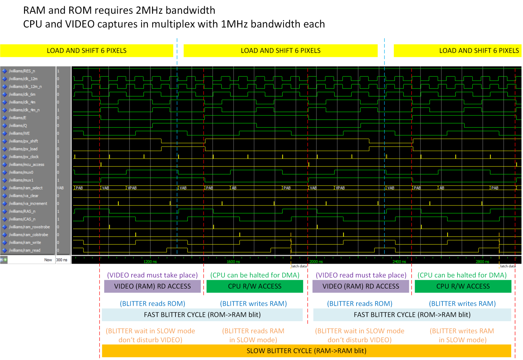
The “spikes” in the waveform are set up on purpose and should just illustrate the relevant time point of certain aspects of capturing adresses for the DRAM or when the blitter or MCU accesses the bus.
This is an simplfied overview of the two memory schemes used on Williams boards to be supported with the FPGA solution:
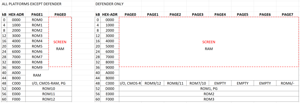
The newer mapping seems to have some advantages in combination with the blitter, as ROM -> RAM blits can be done very fast without any bank switching.
Step three:
The final step is to put everything together and implement it on a FPGA platform.
My preferred boards are from Digilent for Xilinx FPGAs, but I also own some no-name and Terasic boards for Altera/Intel FPGAs, I’d like to map my designs, if I have some time left.
I finished the first setup for the BASYS3 development platform from Digilent. It is still in an early phase, but I think “good enough” for a first release.
Be aware, following features are incomplete or not fully tested:
- the sound board is not yet included
- the interface board is incomplete, game control is not fully/correctly mapped (needs probably also some more configuration options)
- I am still searching for a good idea how to map some game control on the FPGA boards in a useful way – at least for testing
- the ROM board I/O is incomplete as well (but not so complicated to map, though)
- only very minimal testing done (run through all attraction screens, “insert” a coin and do some minimal player movement until game was over and the credit was used up).
- Following ROMs I were tested:
- Defender (blitter off, stargate mode off)
- Stargate (blitter off, stargate mode on)
- Robotron (blitter on, stargate mode on)
- Joust (blitter on, stargate mode on)
- A blitter test program I found at seanriddle.com
Download here at your own risk, please consider the individual licenses/disclaimers in the archive file and consider it is an ALPHA RELEASE (<80kB):
Updated version, for BASYS3 with PMOD AMP1 connected to the lower JB port, with additional features:
- Preliminary 6502 CPU included
- Early release of sound board included
- Simple 1-bit DAC included for PMOD AMP1
- Control input as found on BASYS3 modified for Robotron (walk or walk with fire)
- Not tested very much (basically just with Robotron yet), so use with care!
Download here at your own risk, please consider the individual licenses/disclaimers in the archive file and consider it is an ALPHA RELEASE (<100kB):
To contact me, check out the impressum. But please read the final comments below before doing so.
Final comments:
Be aware that this web page and the code found here are not at all for beginners. I don’t provide turnkey solutions one simply puts on the FPGA board and starts playing. My focus is to create more FPGA code from old arcade PCB boards, so I release just the most relevant code you need to import to a FPGA development environment, not more. You may even add more constraining or do other improvements to get a stable result on your specific FPGA board.
There are several projects out there focussing on providing such projects in a common environment (e.g. fpgaarcade.com), using nice GUIs and so on. This is not my focus.
If you are willing to learn how to use such “bare metal HDL code” I provide here, start with some basic tutorials and books on FPGA design, download the BASYS3 reference manual, try out some of the examples provided e.g. by Digilent and implement some simple examples yourself. There is so much information on the web, I assume you are familiar with common tools to search for these topics.
These are just some links to Digilent resources as starting point:
- Digilent offers a large amount of free trainings and tutorials, start here: https://reference.digilentinc.com/learn/tutorials/start
- Older ISE tutorials (still good to learn the basics in VHDL and Verilog design): https://learn.digilentinc.com/classroom/tutorials/
- More specific, here is the BASYS3 reference manual (only make sense to read if you know the basics): https://reference.digilentinc.com/reference/programmable-logic/basys-3/start
- Here is the BASYS3 getting started manual (again, only make sense to read if you know the basics): https://reference.digilentinc.com/learn/programmable-logic/tutorials/basys-3-programming-guide/start
To be fair, here are also some links from other companies:
- Here is the entry point for Terasic tutorials: https://www.terasic.com.tw/cgi-bin/page/archive.pl?Language=English&CategoryNo=49
- Also distributors like Digikey offer information material, like this introduction to FPGAs: https://www.digikey.com/en/articles/fundamentals-of-fpgas-what-are-fpgas-and-why-are-they-needed
Feel free to search for other resources, I would recommend to look mainly on professional and university web sites to be “safe” and learn the proper and correct things from experts. There is so much crap on the web as well, especially on platforms like Youtube and Facebook, but I am sure you are aware of that…